Intel Xe DG1 GPU is shipping and will release this year

So while TSMC is certainly planning for volume production within 2 years, it's more likely to be 3 before we see any large chips on the process.
I think that's a reasonable estimate. To return to the OPs question about physical limits on lithography, it appears that the GAA transistors debuting at N2 will keep us going for at least another several years.
 
Same. I'm also plesantly surprised with Intel's commitment to low-end and low-mid tier gaming GPUs, segments that Nvidia and AMD have pretty much abandoned. I'd like to see these companies return to launching GPUs in these segments as parts of current lineups, and with the same feature set as high end models.

Or maybe thats the only market segment theyre able to properly compete with at the moment... Like they always have with integrated graphics....Especially when the completion has "abandoned" it, minus amd's integrated and nvidias low end laptop dedicated gpus
Of course.

Funny they always had integrated graphics and it will be the biggest thing cannibalizing their new dedicated videocard sales
 
Last edited:
Yeah, however the point is, who's to blame for that? That's because AMD and Nvidia keep selling GPUs with 10+ year old technology in the $50-$100 price range. But it wasn't always like this. Remember Radeon 9200? Geforce 6200? 8400GS? All current-gen budget cards at their time, with the same feature set (or almost minus a few things) as higher-end cards and offered pretty interesting bang for buck.

It became a pointless segment because AMD and Nvidia's business model made it pointless on purpose.

"interesting bang for buck"? Is that some type of fancy double speak for hot expensive garbage? IIRC when those cards came out, they were terrible value for the money, the people buying them generally just needed it for extra displays so they could care less about the "feature set" and just wanted a new reliable readily available cards with warranty vs. buying less expensive and questionable used garbage on the used market

Not to mention during or after the 8400GS, integrated graphics were starting to flesh out and become decent too.

Nope, I tell from experience because I've owned the cards I mentioned.

The Radeon 9200 and Geforce 6200 were great value for a broke high school kid. They were only "hot garbage" if you were already full PC master race and used to playing everything at 60 fps in ultra settings, and wouldn't be content with anything less.

As for the 8400GS, I had purchased it as a stopgap card to use for just a few months when I was gradually building a new PC in 2008, while saving money for a 9800 GTX+ (top single GPU card at the time) and 1440x900 LCD monitor. All I needed was a card that would provide me video output, since the motherboard didn't have integrated graphics or an AGP slot to reuse the card from my old PC, and I wasn't expecting anything more from it.

However when I tested a few games I was surprised with the 8400GS performance. I concluded that if I was a casual gamer and content enough to play the latest games at 1024x768 or 1280x720 resolutions and high settings + 30 fps or medium settings + 60 fps, the 8400GS would've been more than enough. Keep in mind my 8400GS was an initial version model (G86 core), I learned that later on Nvidia launched refresh versions of the 8400GS (rev2 and rev3) that actually are completely different GPUs and much weaker.

Now, the Geforce FX 5200 and 7200GS, those really were dogs. I'd have agreed with you if you were talking specifically about these 2 cards.
 
We are approaching the limits, but they're still some way off. TSMC are currently working on improving N7, while developing N5 and N3 at the same time. The latter is targeted to have a die density 3 times that of N7, although it won't be ready for volume production for another 2 to 3 years.

Samsung are also working on similar improvements:

SFF2019-1%20%289%29.jpg


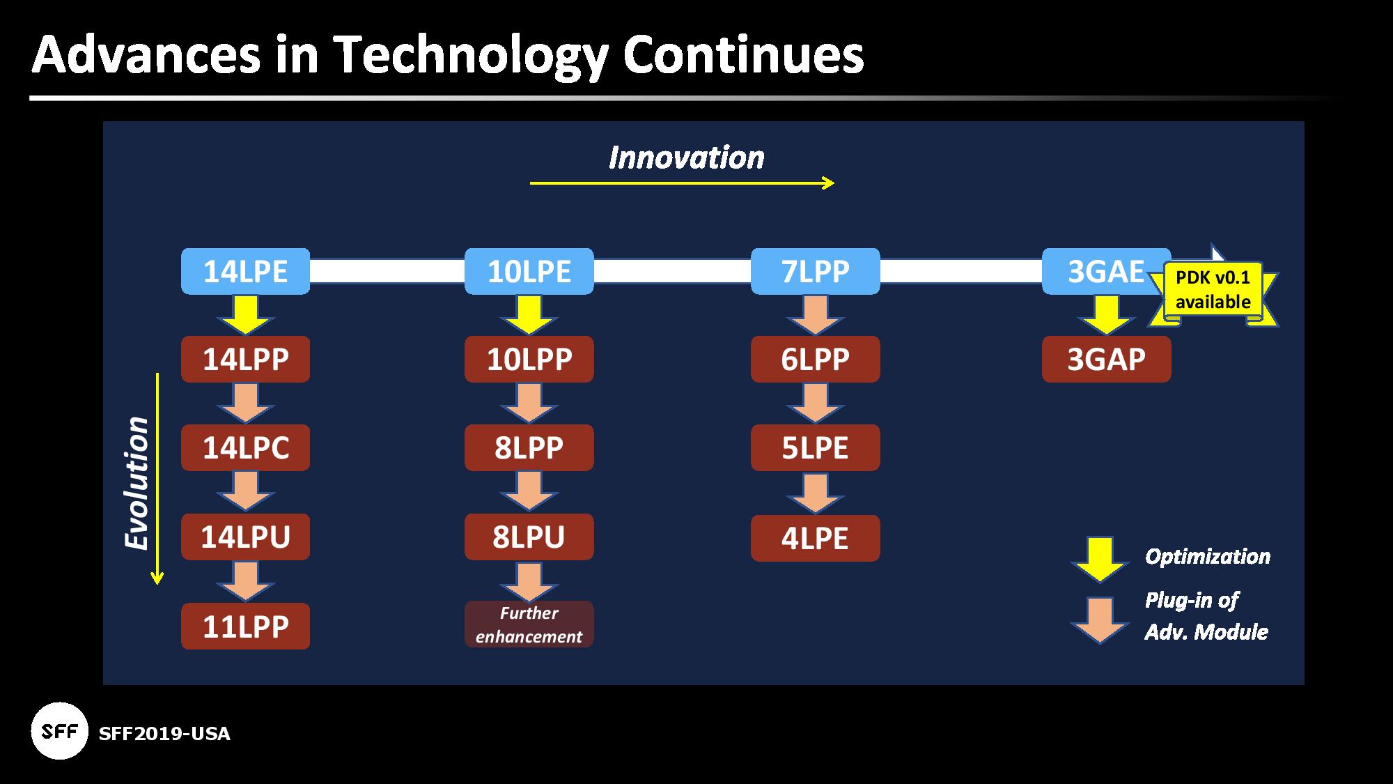
Nvidia's GA102 is made on the 8LPP node, so if they plan on sticking with Samsung, there's clear scope for future monolithic designs to continue the current trend of 'more of everything.'

What kind of chip could one have with 3 times more logic density than seen in the GA102? For the same sized die, that would give you a transistor count of over 80 billion (the GA102 is 28.3b, the GA100 is 54.2b), so even though we're not going to get anywhere near that level anytime soon, it shows that the limits are nicely some distance ahead in the future.

Thank you. I've been reading lots of old PC publications from the late 1980s and early 1990s (mostly the old issues from BYTE and PC Magazine available on Google Books), and there's lots of talk about chip miniaturization.

Most articles from that era on the subject said that chips below 800nm (or 500nm, or 250nm, or 100nm, depending on whom you asked) would be impossible because of quantum mechanics. For them it wasn't a matter of miniaturization engineering - they made clear that from a pure engineering standpoint these chips were possible, but quantum mechanics interference wouldn't make them feasible. They wouldn't run stable. I wonder how chip companies got around this.

Maybe we'll be using chips below 0.1nm eventually.
 
Last edited:
Most articles from that era on the subject said that chips below 800nm (or 500nm, or 250nm, or 100nm, depending on whom you asked) would be impossible because of quantum mechanics... I wonder how chip companies got around this.
A few advances enabled it, but the largest was the shift away from planar transistors into multigate designs, such as the FinFET (and the upcoming GaaFET).

Also, when you read those old articles, remember that the node names we use today are essentially pure marketing. TSMS's "7nm node" is really something more like 20 nm.
 
Back