Forward-looking: As manufacturers search for ways to extend the life of Moore's Law, building transistors only a few atoms thick – called 2D Materials – could be a path forward. Researchers are trying to navigate the obstacles facing 2D transistors as new studies propose multiple methods.

A recent MIT paper proposes a new method to "grow" 2D transistors on top of wafers, potentially speeding the production of ultrathin computing materials. The study claims to solve the heating and assembly problems of other methods, possibly opening new avenues for semiconductors.
Manufacturers like Intel, Samsung, and TSMC continually find ways to make ever-smaller transistors to guarantee ongoing increases in processing power each year. TSMC and Samsung have started 3nm semiconductor production as Intel looks forward to counting transistor size in Angstroms, while talk has also shifted to "2D materials" that are only a few atoms thick.
Researchers at the McKelvey School of Engineering at Washington University in St. Louis proposed a breakthrough in January, enabling the growth of 2D materials at the wafer scale, thus opening up their industrial applications. A more recent MIT study seeks to make the process fast enough to make 2D materials viable for a wide range of products.
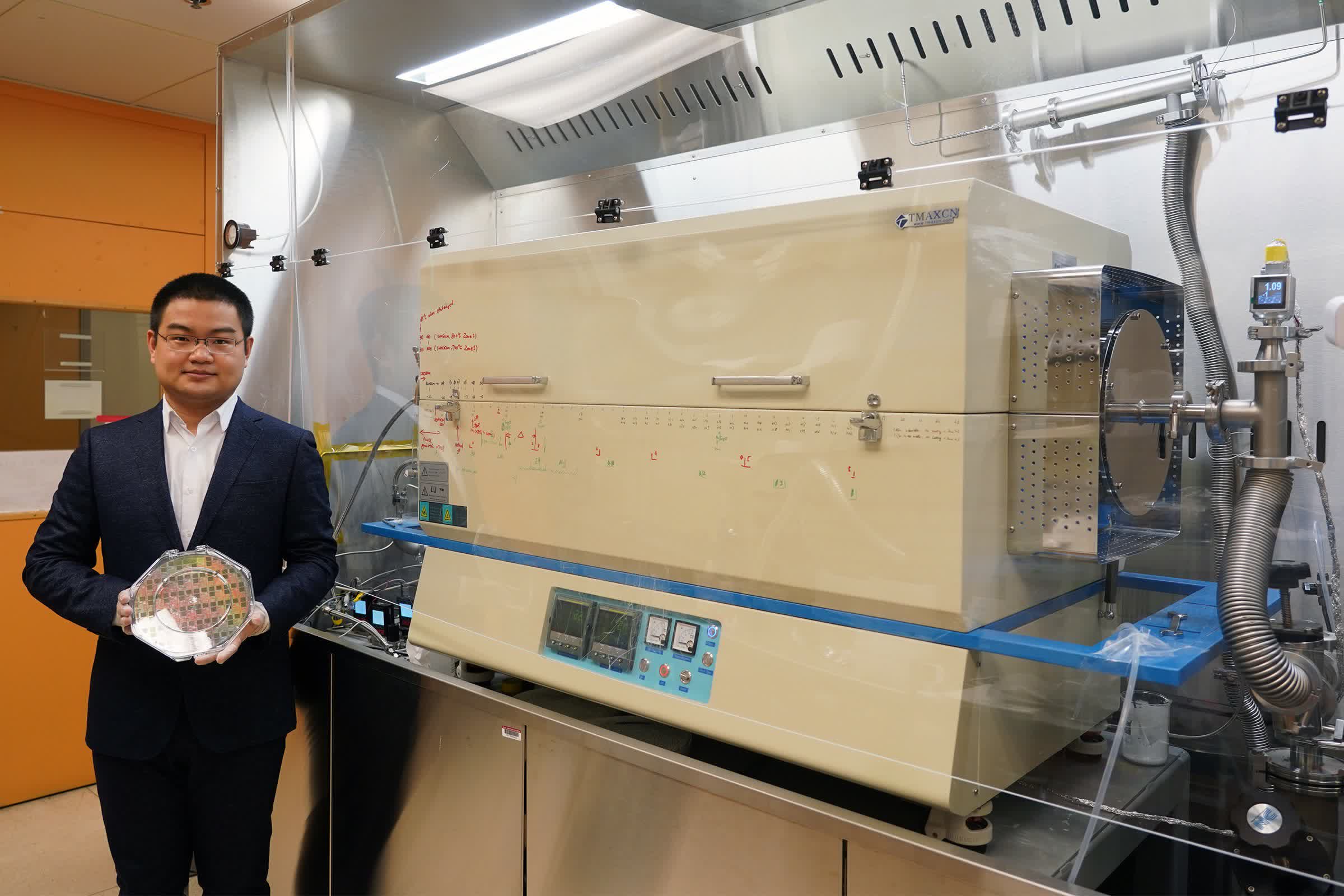
One problem with building the 2D material molybdenum disulfide is heat. Growing some of its components requires temperatures over 550 degrees Celsius, but silicon wafer circuits start decaying beyond 400. Normally, manufacturers graft the 2D material onto the wafer after its production, often leading to imperfections.
The researchers instead grew the material directly onto the wafer with a new kind of kiln that separates part of the cooking process. A high-temperature zone processes the sulfur, after which it flows into the lower-temperature region where the molybdenum and the wafer are kept below 400C. The system leads to more uniform surfaces and faster production.
While the prior method could take an entire day to grow a layer, the new technique can grow a layer in under an hour. The improvement could enable growth across larger surfaces, and the researchers plan to explore stacking layers.
A possible next step would be to grow the transistors on flexible surfaces like polymers, textiles, and paper. If the process is successful, it could lead to integrating semiconductors into things like physical books or clothing.
https://www.techspot.com/news/98556-mit-researchers-unveil-faster-method-growing-2d-transistors.html