The big picture: If successfully scaled to industrial production, these chips could extend Moore's Law into the atomic domain by enabling far greater component density without incurring unsustainable energy losses. While mass production is still several years away, the breakthrough marks the closest two-dimensional materials have come to commercial viability.
Researchers at Fudan University in Shanghai have developed the world's first fully functional memory chip made entirely from two-dimensional materials. The achievement, published in Nature, demonstrates that atomically thin semiconductors can be successfully integrated with conventional silicon systems, a milestone once thought to be decades away.
The Fudan team, led by researcher Chunsen Liu, built the device using a fabrication process known as ATOM2CHIP. The technique enables a sheet of molybdenum disulfide just a few atoms thick to be grown directly on top of a standard 0.13-micrometer CMOS silicon chip. The result is a hybrid system that combines a 2D NOR flash memory array with a traditional CMOS controller, effectively bridging experimental nanomaterials research with established chip manufacturing processes.
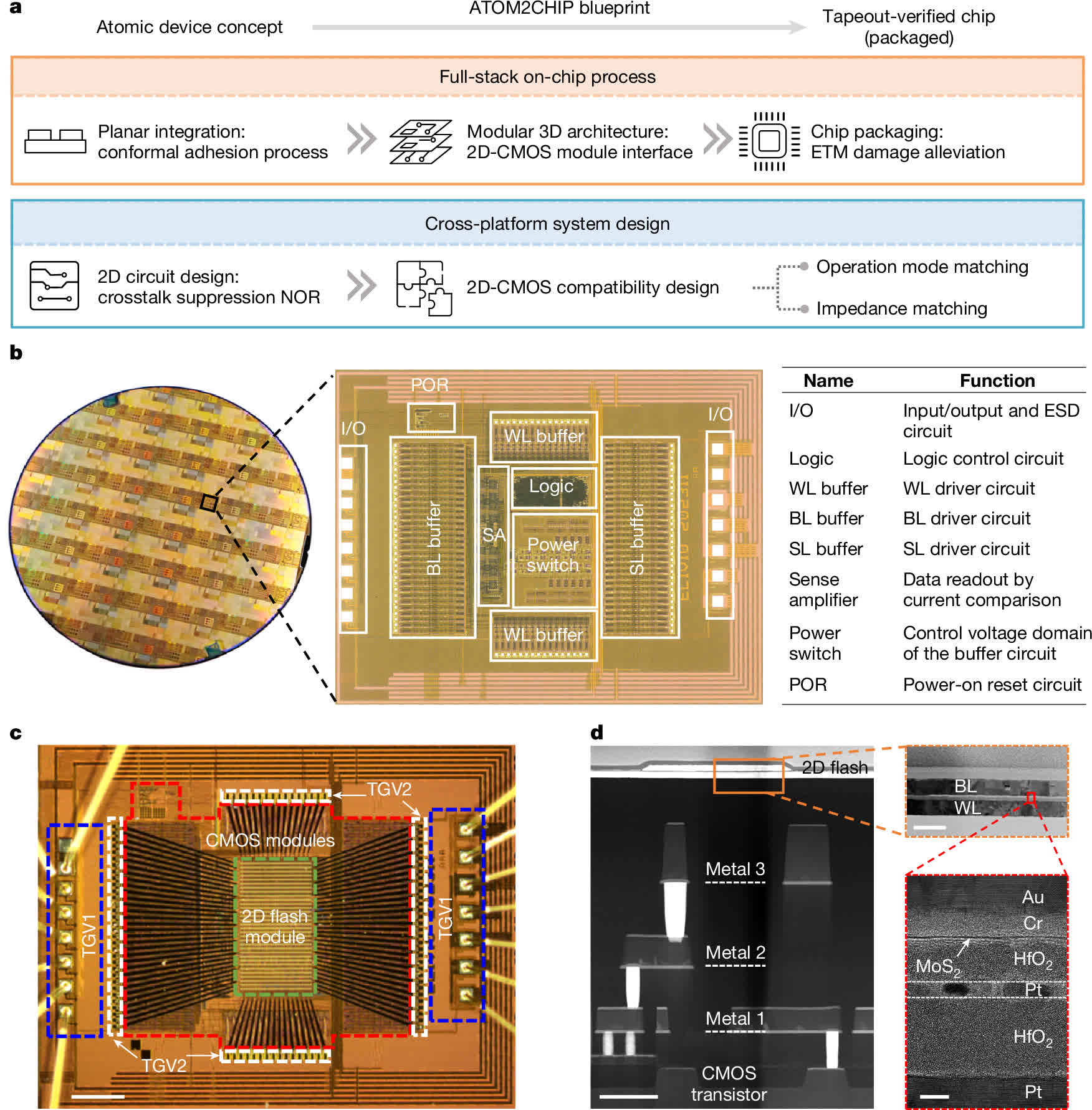
A 2D flash memory chip with ATOM2CHIP technology.
The resulting chip is notable not only for its design but also for its performance. It achieved a 94.34 percent yield during full-chip testing, placing it on par with standard industrial silicon fabrication. Each bit consumes just 0.644 picojoules of energy, dramatically lower than conventional flash memory. The device demonstrated write and erase speeds of 20 nanoseconds, data retention of up to a decade, and endurance exceeding 100,000 write cycles. Operating frequencies reached five megahertz – a modest figure by modern computing standards but a major leap forward for two-dimensional flash systems.
One of the biggest obstacles to such integration has been structural compatibility. Even the smoothest silicon wafer is rough on the nanometer scale, posing a risk to ultrathin films that can tear or buckle when applied directly.
The Fudan team overcame this by developing a conformal adhesion technique that allows the 2D material to spread across these microscopic peaks and valleys without fracturing. The ATOM2CHIP process also incorporates a protective encapsulation architecture tailored for two-dimensional electronics, shielding the atomic layers from heat and electrostatic discharge.
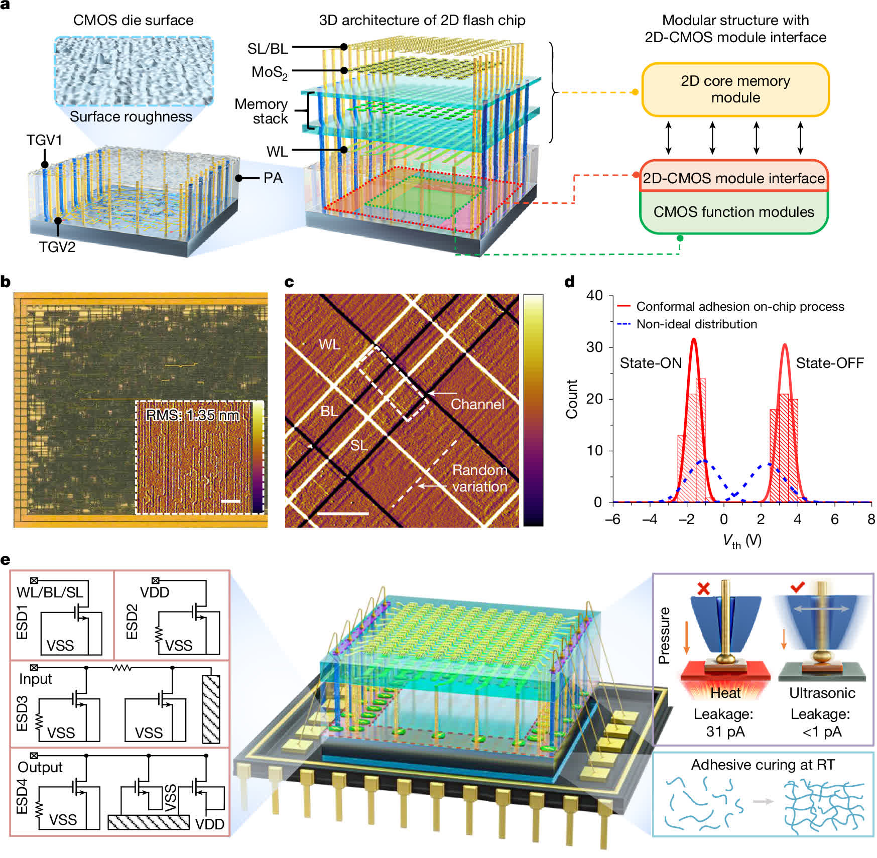
The 3D architecture of the fabricated 2D flash chip.
To make the two-dimensional layer functional within a complex silicon environment, the researchers developed a custom "cross-platform" system that links the 2D memory array directly with the CMOS control logic. This architecture enables instruction-level operations, random access, and 32-bit parallel data handling – essential capabilities for modern memory devices.
The team describes the framework as an early step toward atomic-scale heterogeneous computing, where ultra-dense, low-power storage arrays are integrated directly atop processing circuits.
This is not Fudan University's first breakthrough in ultrafast memory. Earlier this year, the same group demonstrated a 2D-based flash prototype that achieved a record-setting program speed of 400 picoseconds, the fastest semiconductor charge-write time ever verified in a laboratory setting. The new chip builds on that success, transforming what was once experimental technology into a functional and scalable system.
According to Liu, integrating emerging materials within standard CMOS architectures could compress innovation cycles that previously took decades. He noted that while earlier semiconductor transitions such as the move from discrete transistors to integrated CPUs spanned more than 20 years, hybrid 2D – silicon systems could reach commercialization much sooner thanks to their compatibility with existing fabrication lines.
The implications for artificial intelligence and data processing are significant. Memory bottlenecks – particularly slow access speeds and high power consumption – remain key constraints on AI hardware, which depends on rapid data exchange between processors and storage units.
Fudan's hybrid chip points toward a future where both speed and energy efficiency improve dramatically without compromising manufacturability. Co-author Zhou Peng suggested that memory products could be the first class of 2D components to reach mass production, as they place fewer demands on the base material yet deliver substantial performance gains.
New 2D memory chip could extend Moore's Law into the atomic era