Forward-looking: Scientists have been looking to create light-emitting silicon for over 50 years. It had become something of a "Holy Grail" in the microelectronics community. Such a discovery would mean faster on-chip communication, lower heat production, and higher power efficiency.
Now researchers at Eindhoven University of Technology (TU/e) have figured out this decades-long conundrum by creating a new hexagonal silicon alloy capable of emitting light. The hexagonal shape is key to creating a direct bandgap that will emit photons.
"The crux is in the nature of the so-called bandgap of a semiconductor," said TU/e project lead Erik Bakkers. "If an electron 'drops' from the conduction band to the valence band, a semiconductor emits a photon: light."
In traditional cubic silicon, the conduction and valence bands are displaced creating an indirect bandgap, so no photons can be emitted. However, it was theorized 50 years ago that alloyed silicon and germanium in a hexagonal configuration would have a direct bandgap. The trick is creating such an alloy.
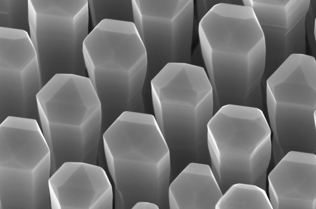
This feat had been impossible until the development of naotubes and wires was discovered. The team was able to create hexagonal silicon in 2015 by growing nanowires from another material and using it as a template to develop hexagon-shaped silicon with a germanium shell.
"We were able to do this such that the silicon atoms are built on the hexagonal template, and by this forced the silicon atoms to grow in the hexagonal structure," said Elham Fadaly, coauthor of the team's paper, which was published in Nature.
The researchers now need to develop a silicon-compatible laser. According to Bakkers, they could have one before the end of this year.
"If things run smoothly, we can create a silicon-based laser in 2020," he said. "This would enable a tight integration of optical functionality in the dominant electronics platform, which would break open prospects for on-chip optical communication and affordable chemical sensors based on spectroscopy."
Since photons are not subject to resistance and have less scatter within the conducting medium, no heat is produced, so power consumption is significantly reduced. Furthermore, the on-chip and chip-to-chip communication speeds could increase by a factor of 1,000 on future photonic silicon. The technology has many applications, including laser-based radar for autonomous vehicles and chemical sensors used in both the medical and food industries.
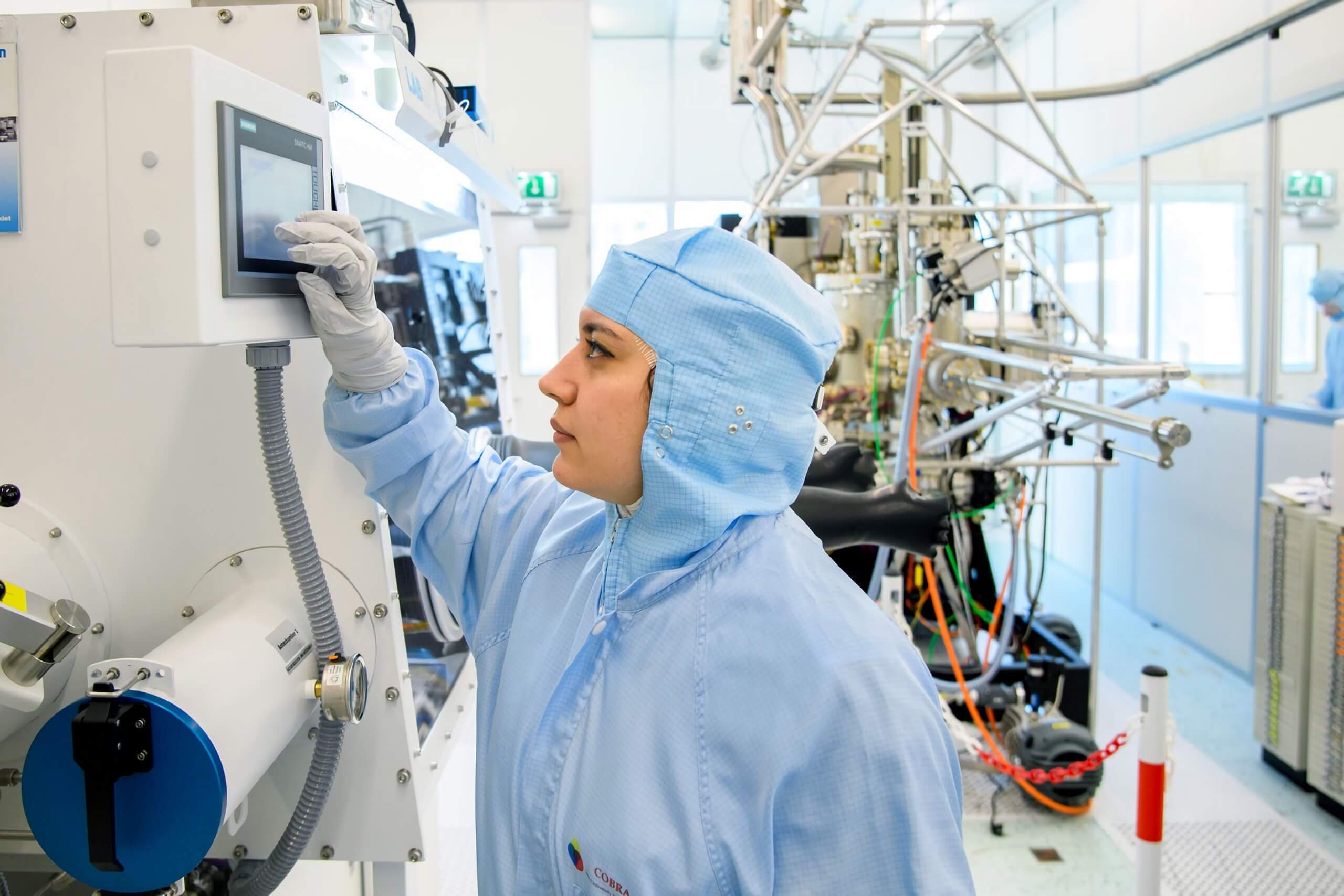
Image credit: TU/e
