Something to look forward to: Today's evolving technologies and processing requirements have driven chipmakers to pursue alternative designs that deviate from standard monolithic die-based architectures. Earlier this week, Taiwan Semiconductor Manufacturing Company (TSMC) announced the formation of the 3D Fabric Alliance to meet those requirements better. The Alliance creates a collaborative effort between industry partners to accelerate 2.5D and 3D chiplet-based product designs, development, and industry adoption.
The 3DFabric Alliance applies the combined expertise of multiple industry partners to create and refine chiplet-based design and packaging technologies. The 19-member alliance, which is expected to expand, spans the entire product ecosystem and includes partners specializing in design, automation, memory, substrate, test, and other areas of the manufacturing process. These members will work together to develop 3DFabric technology specifications according to TSMC-established rules and standards.
The Alliance is part of TSMC's larger Open Innovation Platform (OIP). The OIP model provides a means for customers and industry partners to collaborate and establish new approaches to shorten integrated circuit (IC) design time. It also aims to improve time-to-volume, time-to-market, and time-to-revenue.
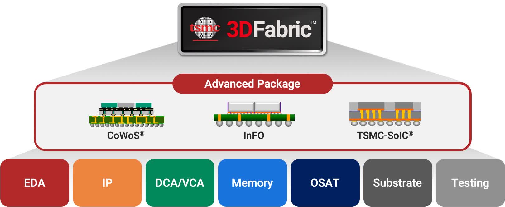
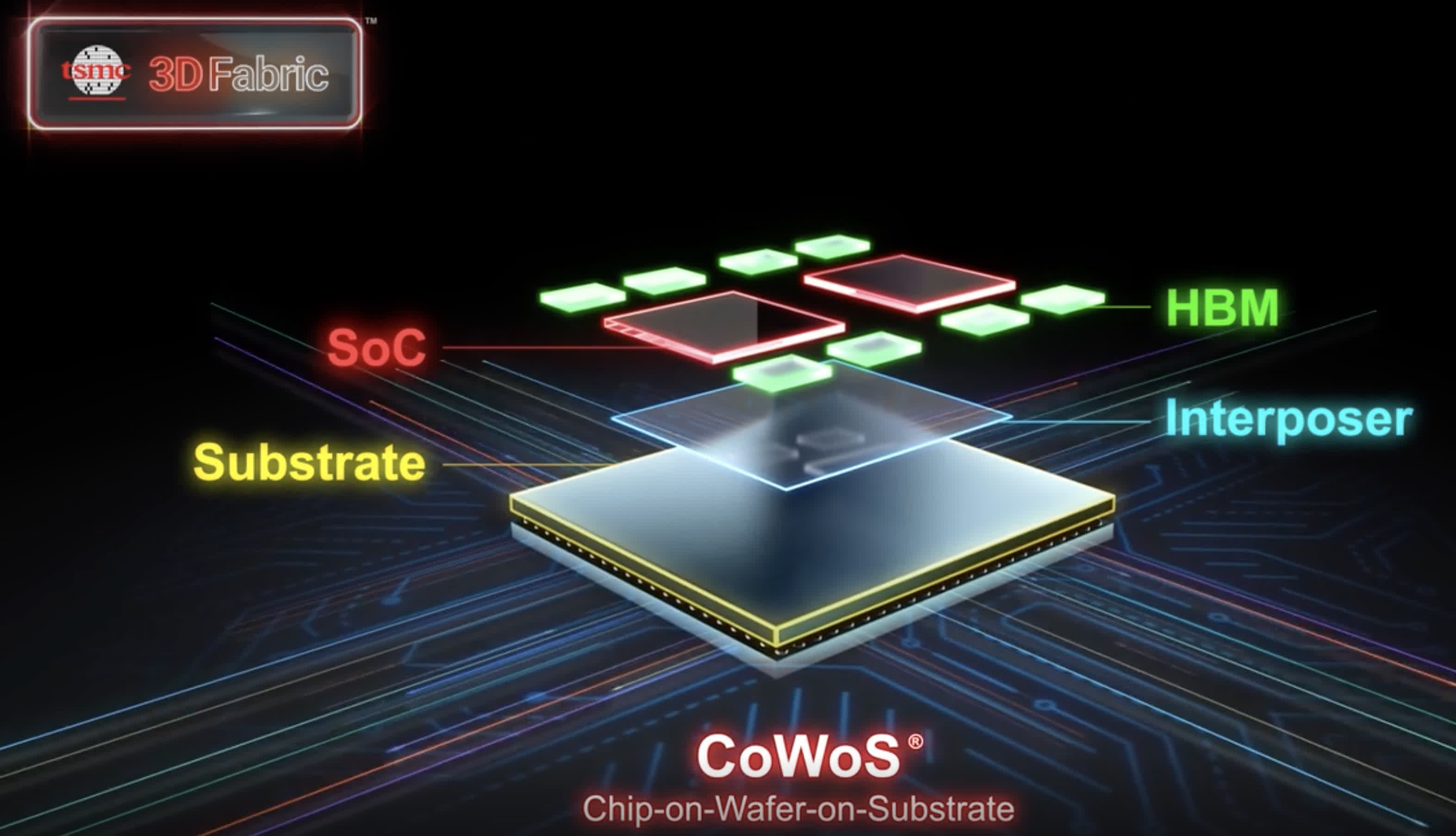
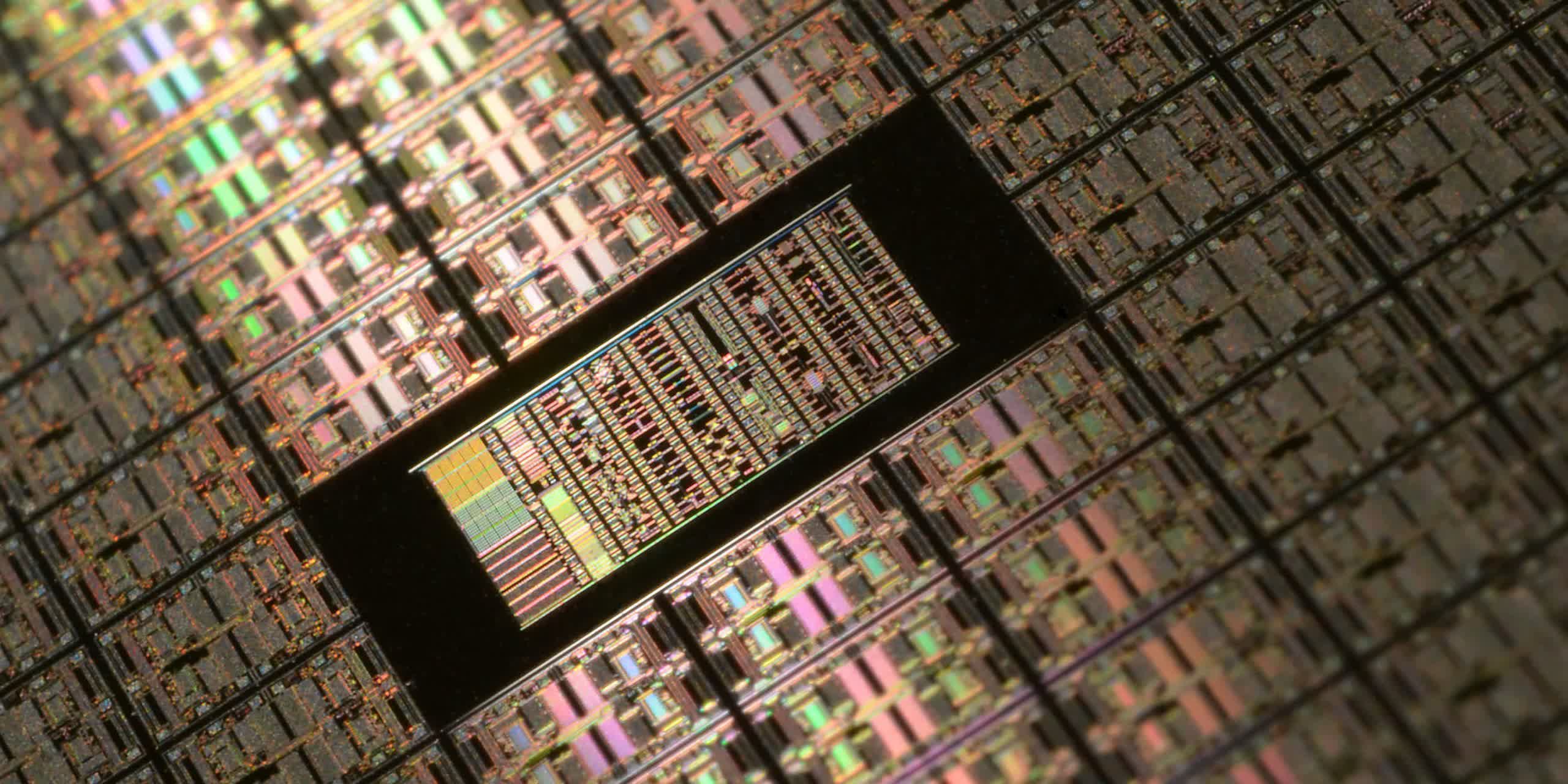
Taiwan Semiconductor Manufacturing Company's 3DFabric is a family of front-end and back-end interconnect technologies designed to increase future computing power and core counts, raise memory and bandwidth ceilings, and enhance overall power delivery. The approach supports TSMC's system on integrated chip services, including chip-on-wafer and wafer-on-wafer die stacking methodologies. This technique uses high-density vertical stacking to increase performance and reduce power consumption. It also allows for better integration of known good dies with chips of various sizes and functionalities, enhances overall scalability, and reduces the footprint and profile of the chip.
The overarching goal of the 3DFabric Alliance is to create standard, interoperable solutions that speed up multi-chiplet design and development efforts for use across all industries. According to TSMC, the role of semiconductors will continue to increase across all sectors due to their use in everything from automotive design and manufacturing to data centers and smart devices. The 3DFabric Alliance's ability to optimize and streamline the design, development, and implementation will help ensure continued innovations for semiconductor technology and everyday products and services that rely on them.

