In a nutshell: TSMC has just announced its entire lineup of 3nm class nodes launching over the next three years. Its new FinFlex tech will give chip designers even more flexibility to optimize each standard cell for the desired power consumption, performance, and density.
TSMC has just unveiled its entire N3 family of process nodes. Chip designers such as AMD, Apple, Nvidia, and even Intel will use these nodes over the next few years to fabricate their bleeding-edge chips.
The Taiwanese company has a total of five different 3nm class nodes. N3 will begin high-volume manufacturing later this year, with the first chips expected to reach customers early next year. N3E will launch later with performance and efficiency improvements, higher yields, but slightly reduced logic density.
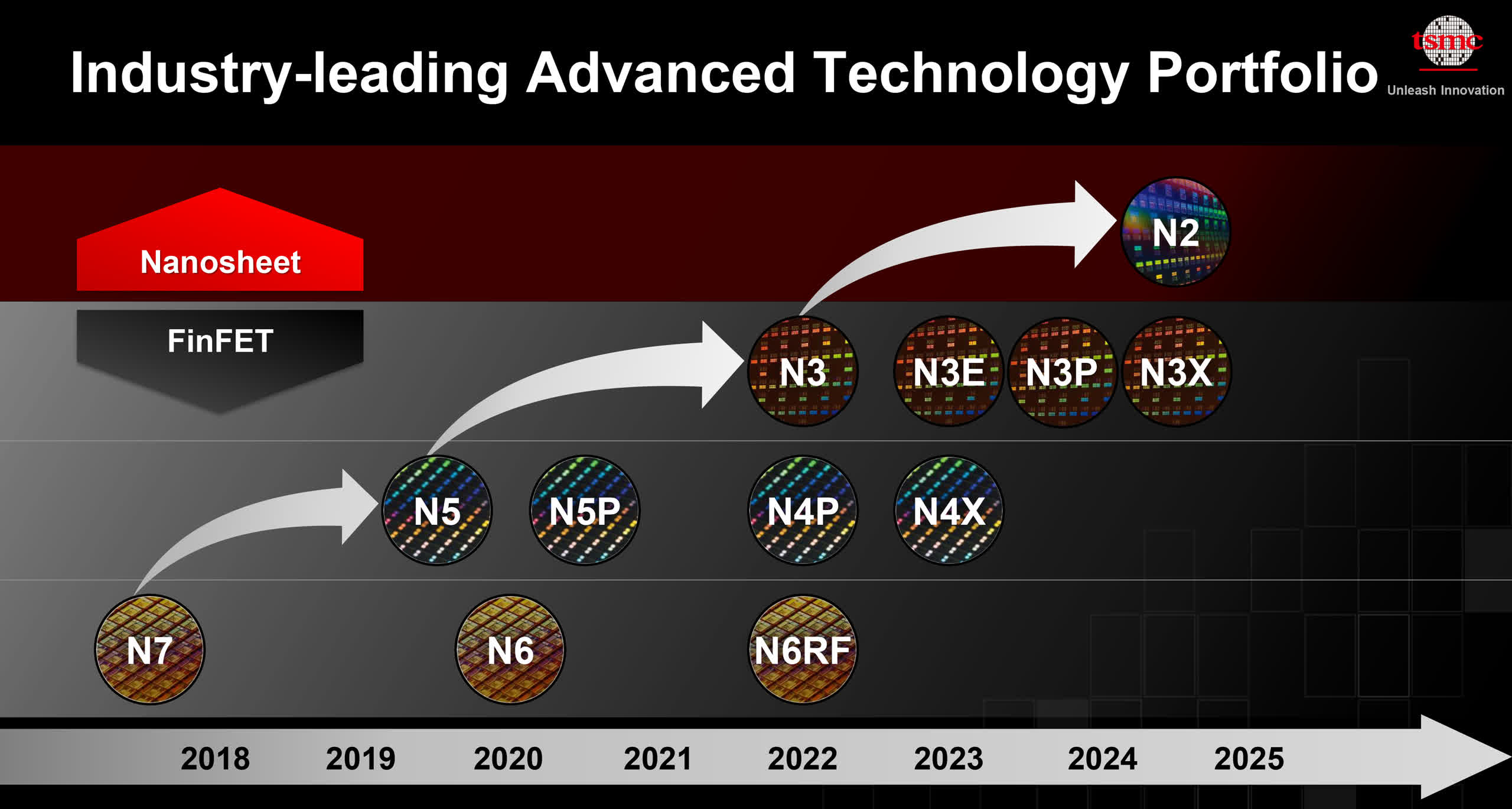
Around 2024, TSMC will bring out N3P, which focuses on performance improvements. N3S, which wasn't featured in TSMC's roadmap, was only briefly mentioned in conversation by SVP Kevin Zhang.
Finally, N3X will come out about a year later and allow for extremely high performance at higher voltages, with efficiency and costs taking the back seat. This approach is similar to the 5nm class N4X process starting volume manufacturing next year.
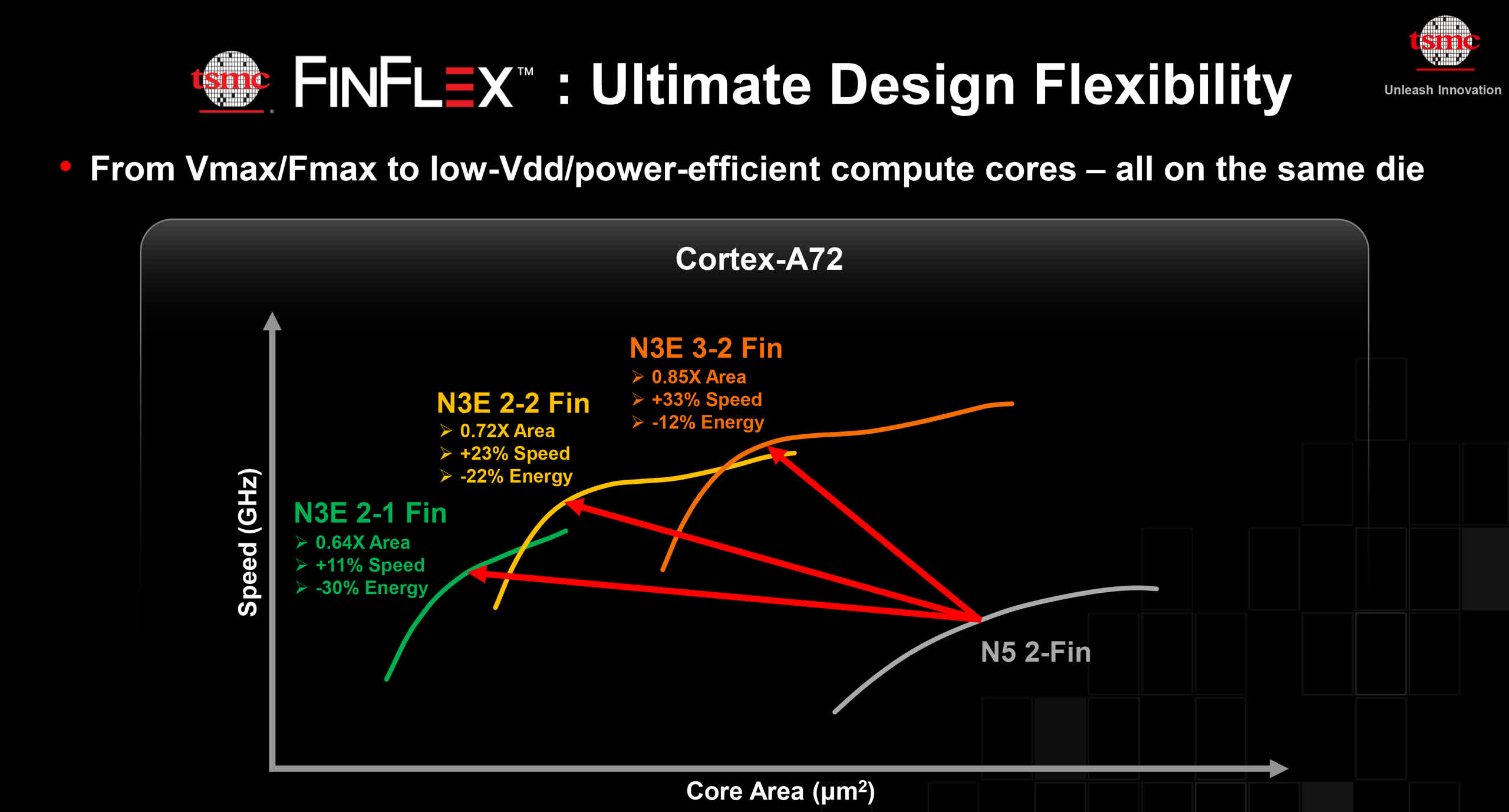
TSMC's N3 and N3E nodes will also support the company's new FinFlex tech. Currently, chip designers have to pick one library for each block within an SoC. With FinFlex, they won't have this limitation and will be able to mix and match different libraries within each block.
They can use 2-1 (double-gate single-fin) FinFETs in some parts in order to reduce power consumption and die size (cost) and opt for 3-2 FinFETs in other areas where maximum performance is paramount. Meanwhile, 2-2 FinFETs provide a balance of size, performance, and power consumption.
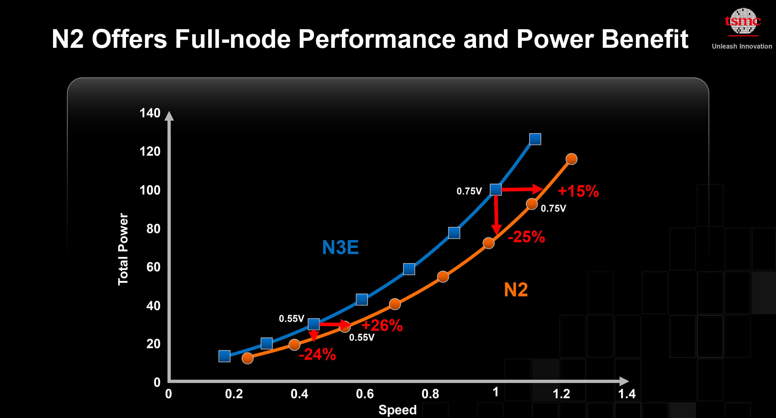
TSMC also mentioned its upcoming N2 process node, which will use gate-all-around field-effect transistors (GAAFETs), with plans to start volume manufacturing in the second half of 2025.
Compared to N3E, it will reportedly draw 25-30 percent less power at the same frequency and allow for 10-15 percent more performance with the same power consumption and transistor count. Meanwhile, chip density will reportedly increase by over 10 percent.
https://www.techspot.com/news/94986-tsmc-announces-handful-3nm-process-nodes-n2-coming.html
