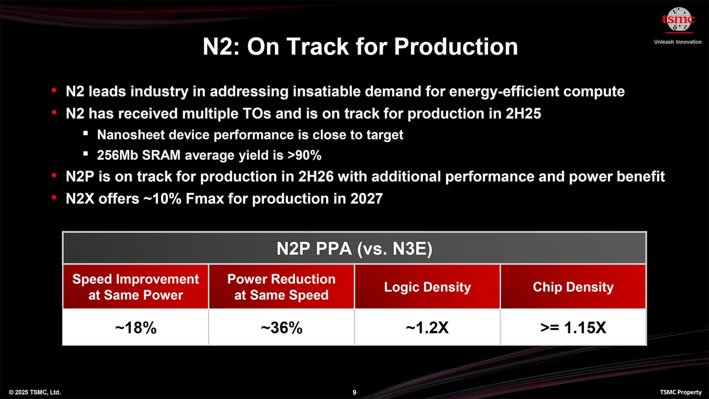
Something to look forward to: TSMC is moving faster than expected to bring its most advanced chip technology to market. The company confirmed that its N2 process node will enter volume production before the end of 2025, as it accelerates both its domestic rollout in Taiwan and a parallel push to deploy the same technology at its Arizona site.
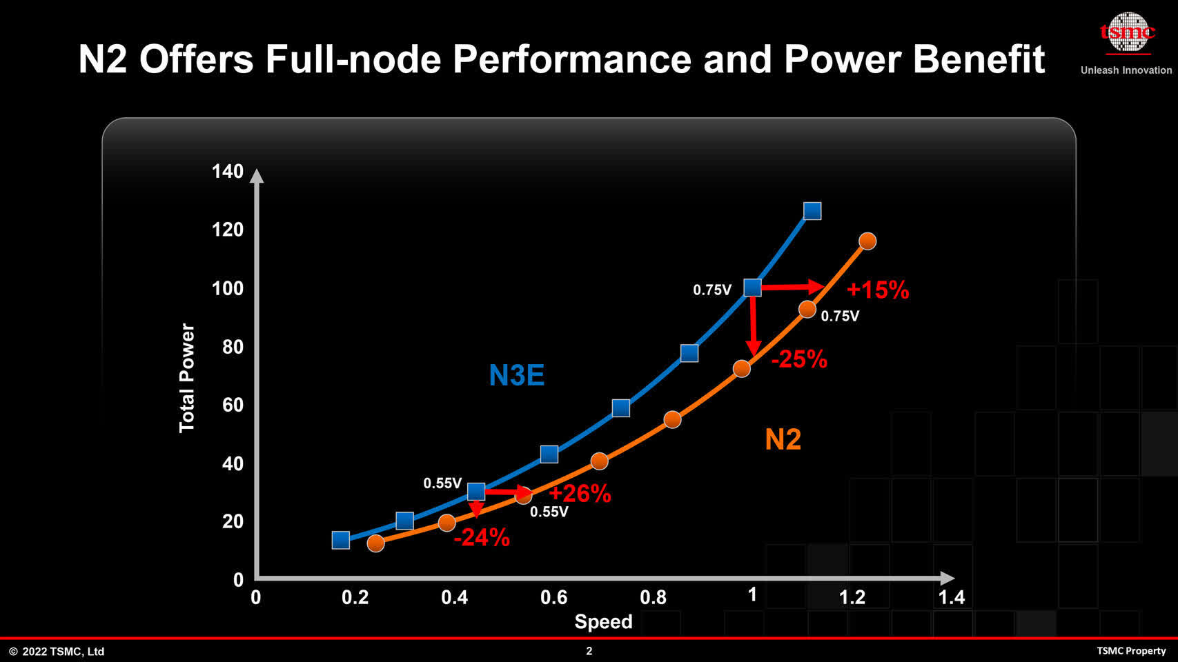
The N2 node introduces nanosheet-based gate-all-around transistors, replacing the FinFET architecture used since the 16-nanometer generation.
Early yields have been strong, according to company executives, with mass production set to ramp up sharply through 2026. TSMC is also developing a next-step process known as N2P, expected in the second half of 2026, to deliver further efficiency gains.
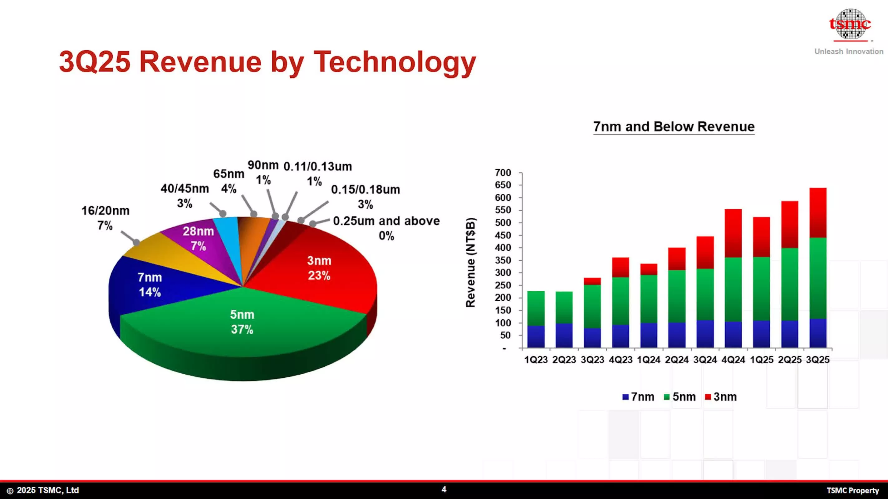
The 2-nanometer milestone coincides with record financial results for the third quarter. TSMC's revenue rose more than 40% from a year ago to $33.1 billion, powered by demand for AI accelerators and premium smartphone chips.
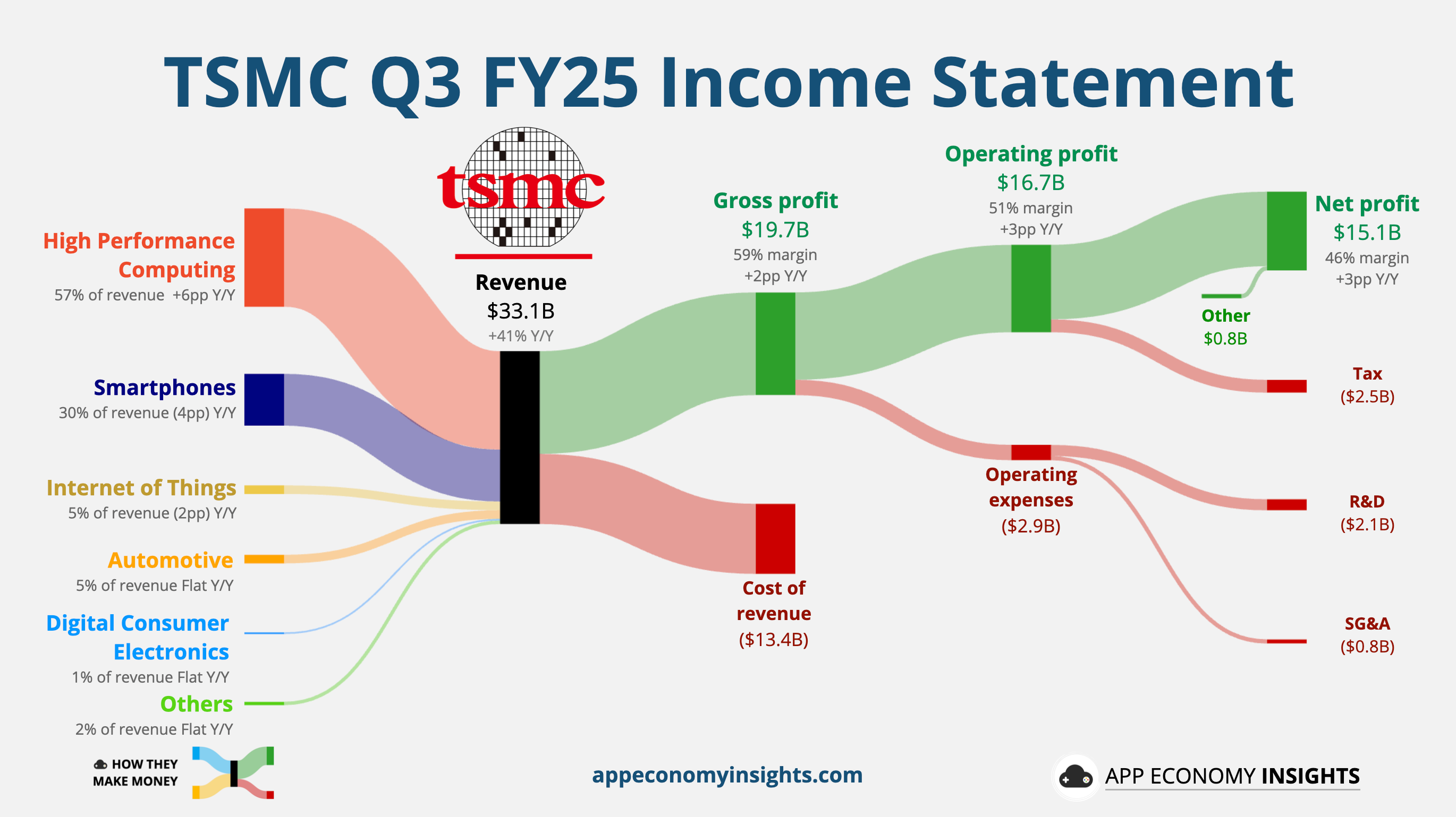
Masthead and income statement graphs credit: App Economy Insights
Advanced process technologies – spanning the N3, N5, and N7 families – made up nearly three-quarters of sales. Company leaders said capital spending will remain aggressive, totaling as much as $42 billion this year, with nearly three-quarters of that directed toward expanding leading-edge manufacturing capacity.
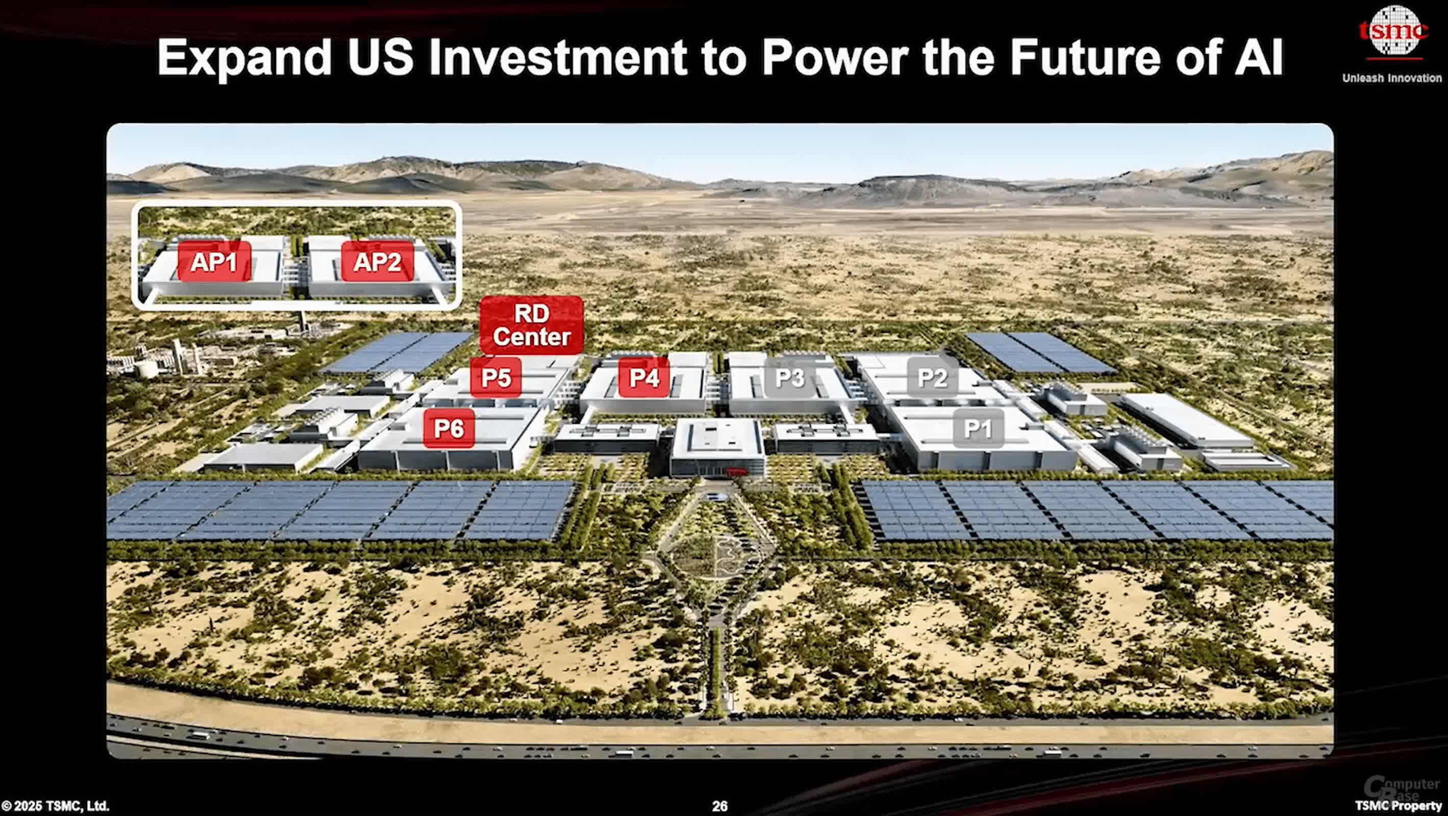
TSMC's Arizona buildout is now central to those investments. The company has already begun producing chips using its N4 process at the first module of Fab 21 near Phoenix and will bring N3 online next. But in an earnings call this week, Chief Executive C.C. Wei said the company will "upgrade our technologies faster to N2 and more advanced processes in Arizona, given the strong AI-related demand from our customers."
That admission marks a major acceleration – N2 production at Fab 21 had originally been expected near the end of the decade.
The twin efforts mark a pivotal moment for the world's largest contract chipmaker as it seeks to meet the surge in global demand for high-performance processors used in AI and advanced computing.
Construction of new modules for N2 and its successor, A16, is expected to begin later this year. When complete, about 30% of TSMC's output from 2 nm-class and more advanced nodes will be produced in the United States.
The company's Arizona site is expected to evolve into a "GigaFab" cluster capable of turning out roughly 100,000 wafers a month, fully integrated with packaging, testing, and local supplier networks.
The shift comes during renewed efforts by US policymakers to secure domestic chip production capacity and lessen dependence on Asian foundries.
Wei underscored that context, describing the Arizona expansion as a step toward creating "an independent, leading-edge semiconductor manufacturing cluster" in the United States. The company is exploring additional land acquisitions around its existing campus to support further expansion beyond its original $165 billion US investment commitment.
TSMC pushes 2 nm manufacturing ahead of schedule, fast-tracks Arizona buildout