The big picture: The announcement highlights how TSMC continues to frame technological progress not just in terms of incremental improvements but also in its ability to deliver manufacturing advances well ahead of commercial deployment. With trial yields already reported ahead of internal timelines, the A14 process signals another inflection point for the industry in pushing semiconductor design past today's technical bottlenecks.
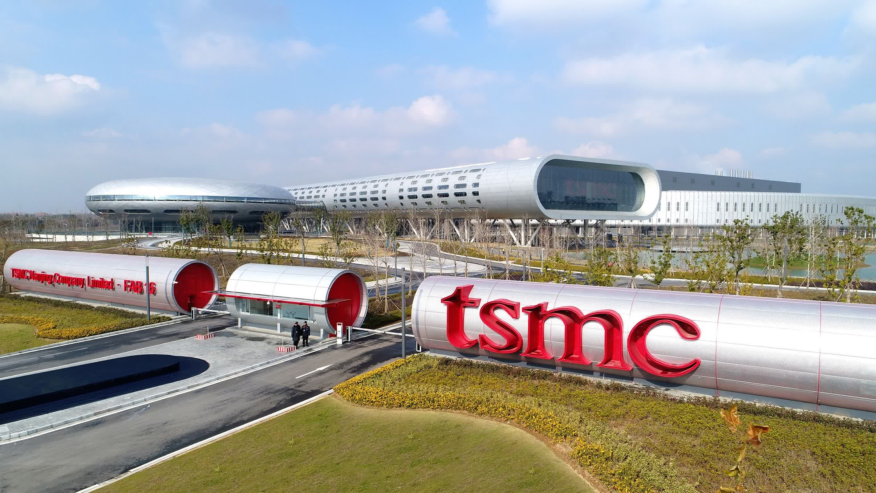
TSMC has released new technical details on its A14 semiconductor process, reporting on both the performance and efficiency gains expected to surpass its 2-nanometer platform. The company said development of the node is ahead of schedule, signaling continued progress even as much of the industry struggles with ramping up current-generation technologies.
According to the company's disclosures revealed by analyst Ray Wang, the A14 process is projected to deliver up to a 15 percent performance increase at equivalent power levels compared with N2. When measured at comparable speeds, the node is expected to reduce power consumption by as much as 30 percent. These improvements will come from the introduction of TSMC's second-generation gate-all-around nanosheet transistors as well as a new design standard called NanoFlex Pro. The updated architecture is designed to provide greater flexibility in balancing power, performance, and density across different design applications.
$TSM's A16 and A14 Process Technology: ""A14 development is progressing smoothly with yield performance ahead of schedule.""
– Ray Wang (@rwang07) September 23, 2025
A16: Integrates nanosheet transistors with Super Power Rail (SPR) and novel backside contacts to deliver industry-leading logic density, power... pic.twitter.com/yi9q5QPnTd
In terms of density, TSMC expects up to a 20 percent increase relative to N2. That figure is critical as manufacturers work to fit more transistors within the same silicon footprint, a key driver of Moore's Law scaling.
The significance of the announcement comes as leading foundries face difficulties with yield, performance, and cost management at advanced nodes. While Samsung and Intel have both outlined roadmaps around future transistor architectures, detailed performance projections have been less forthcoming. Intel's 14A node, for instance, has been placed on its long-term roadmap, but yield data and efficiency metrics have yet to be specified publicly.
TSMC's progress places the Taiwanese firm several years ahead of rivals in signaling readiness for post-2nm development. The company said A14 is targeted for production in 2028, extending its lead in advanced process technology and maintaining its position as the dominant supplier to leading chip designers.
The potential impact of A14 is expected to reach across consumer and enterprise markets. Major customers such as Apple, Nvidia, and AMD remain closely tied to TSMC's roadmaps, with the shift to thinner process nodes shaping product performance, efficiency, and competitiveness in smartphones, data centers, and artificial intelligence hardware.
TSMC reports progress on A14 node with 15% performance boost and 30% power reduction