
Looking ahead: As AI systems push deeper into high-density compute, the bottleneck is no longer just processing power – it is heat. SK Hynix is targeting that constraint with a new memory packaging approach designed to cool one of the hottest regions in the system.
SK Hynix has introduced iHBM, a high-bandwidth memory packaging solution that changes how and where heat is managed inside the package. Rather than relying on conventional methods that pull heat away from the chip after it accumulates, SK Hynix is placing cooling structures directly at the source.
That source is the Die-to-Die Physical Layer, or D2D PHY – the high-speed link between the HBM stack and the AI processor. This interface moves enormous volumes of data, often reaching terabytes per second in high-bandwidth configurations, and generates significant heat in the process.
The combination of switching activity, leakage effects, electrical resistance, and constant data flow turns this layer into a persistent hotspot, especially under sustained AI workloads.
SK Hynix's solution is to embed what it calls Integrated Cooling Elements, or ICEs, directly into that interface. These are electrically isolated, thermally conductive silicon structures built into the D2D PHY itself, dissipating heat at the point of generation rather than after it has spread through the package. The company says the approach reduces thermal resistance by more than 30%.
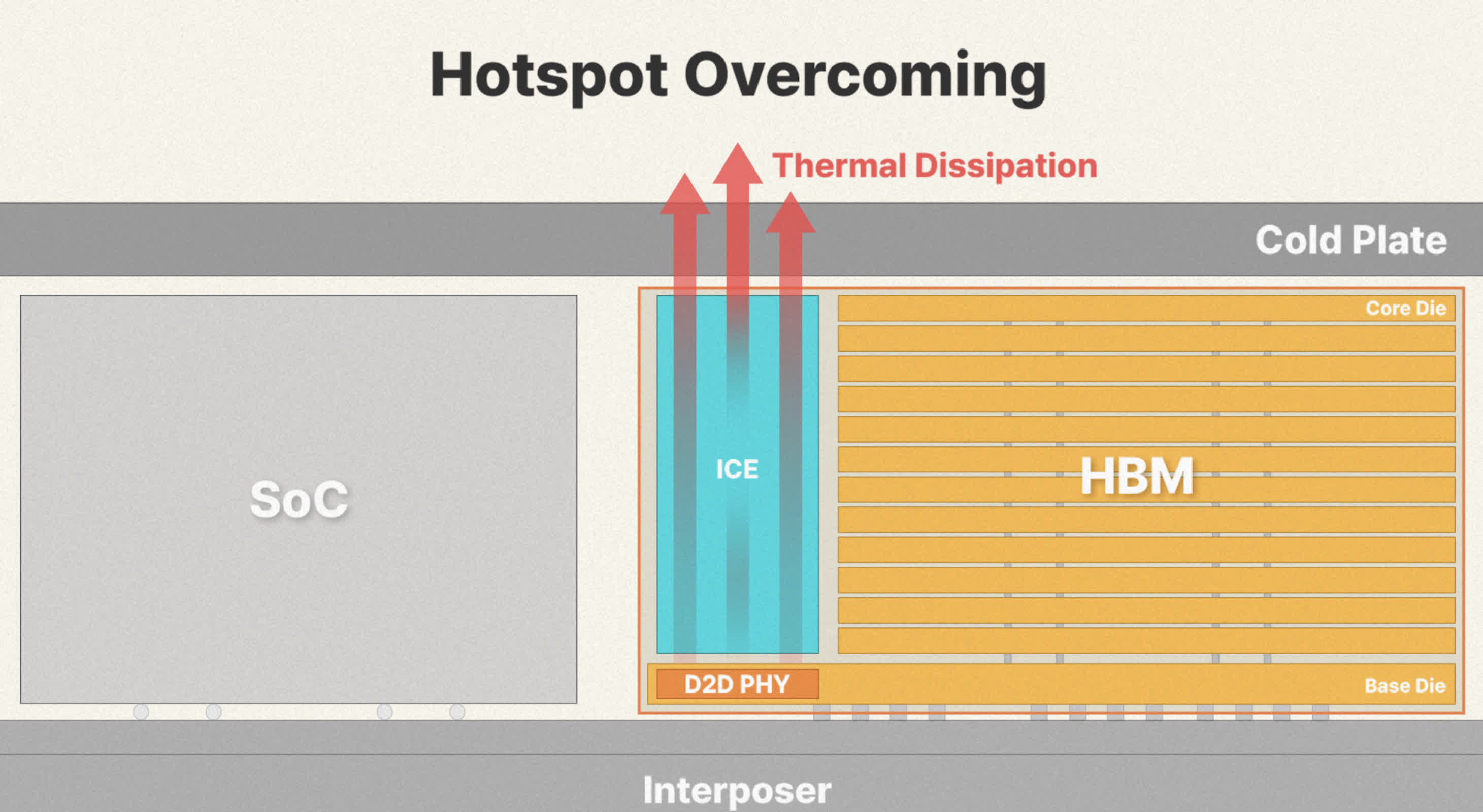
That reduction matters because thermal buildup in this region has a direct impact on performance. When temperatures climb too high, systems automatically throttle – lowering clock speeds and voltages to prevent damage. In AI data centers, where chips are expected to run continuously under heavy load, those slowdowns can significantly affect throughput.
The issue is tied closely to how HBM is designed. Unlike conventional memory, HBM stacks multiple DRAM dies vertically and places them close to the processor using a silicon interposer. This layout improves bandwidth and reduces latency, but it also concentrates heat into a very small area. The processor already generates a lot of heat, and the nearby memory stacks add to it.
What iHBM changes is the idea that cooling has to happen outside that processor-to-memory interface. By adding a direct heat path inside the interface layer, SK Hynix is trying to keep heat from building up there in the first place. The goal is not just better cooling, but more stable performance under sustained workloads.

The company positions iHBM as a stepping stone toward future memory generations, including HBM5, where taller stacks and faster data rates will drive thermal demands even higher. Without packaging-level interventions, those advances risk being constrained by heat before they are constrained by bandwidth or compute.
SK Hynix also notes that the design does not require a manufacturing overhaul. The iHBM structure can be produced using its existing wafer-level packaging process, built on the Mass Reflow Molded Underfill (MR-MUF) technology already used in current HBM products. It is also compatible with existing system-in-package configurations, lowering the barrier for customers to adopt it without rearchitecting their systems.
The shift reflects a broader change in how performance gains are being pursued in AI hardware. As scaling compute alone becomes more difficult, improvements are increasingly coming from how components are integrated and managed at the physical level. In that context, memory is no longer just a supporting component, but it is becoming a decisive factor in whether systems can sustain peak performance at all.