In brief: Samsung is adding a new set of memory technologies to its AI strategy, using wafer bonding and 3D stacking to push bandwidth, density, and energy efficiency beyond what current high-bandwidth memory and NAND technologies can deliver.
At the Future of Memory and Storage 2026 conference in Santa Clara, California, the company laid out a roadmap built around three main technologies: a new Bonding V-NAND architecture with more than 400 layers, a concept for vertically stacked high-bandwidth memory called zHBM, and a next-generation NAND approach called zNAND-O. These technologies target both large-scale AI training workloads in data centers and edge AI applications that require low latency and tight power controls.
A key part of that strategy is zHBM, a new way of arranging high-bandwidth memory. In today's systems, HBM usually sits next to AI processors. zHBM instead stacks HBM directly on top of AI accelerators, placing the memory above the compute. This design shortens the physical distance data has to travel between the processor and memory, which is intended to increase bandwidth and improve power efficiency for large-scale AI training and inference.
Samsung said a next-generation interface system using zHBM is expected to deliver about eight times the performance of HBM5. With wafer bonding, the company believes zHBM can achieve more than 10 times the memory density of HBM5 while improving energy efficiency threefold and cutting thermal resistance by more than half. The goal is to make high-capacity, high-bandwidth systems more stable and easier to cool.
The zHBM concept also adds more flexibility to AI hardware design. It supports customer-specific layouts, allowing customized IP to sit in the layer between the memory stack and AI accelerator. That layer can be used to expand memory capacity or add logic tailored to particular AI workloads.

zNAND-O is a high-performance NAND solution built on Samsung's V-NAND technology and aimed at edge AI. It is in development in four- and eight-layer versions. The company describes it as combining high space efficiency, improved input/output performance, and low latency to support real-time, data-intensive AI applications closer to where data is generated. That puts zNAND-O somewhere between traditional mass-storage NAND and memory products designed specifically for fast inference and local processing.
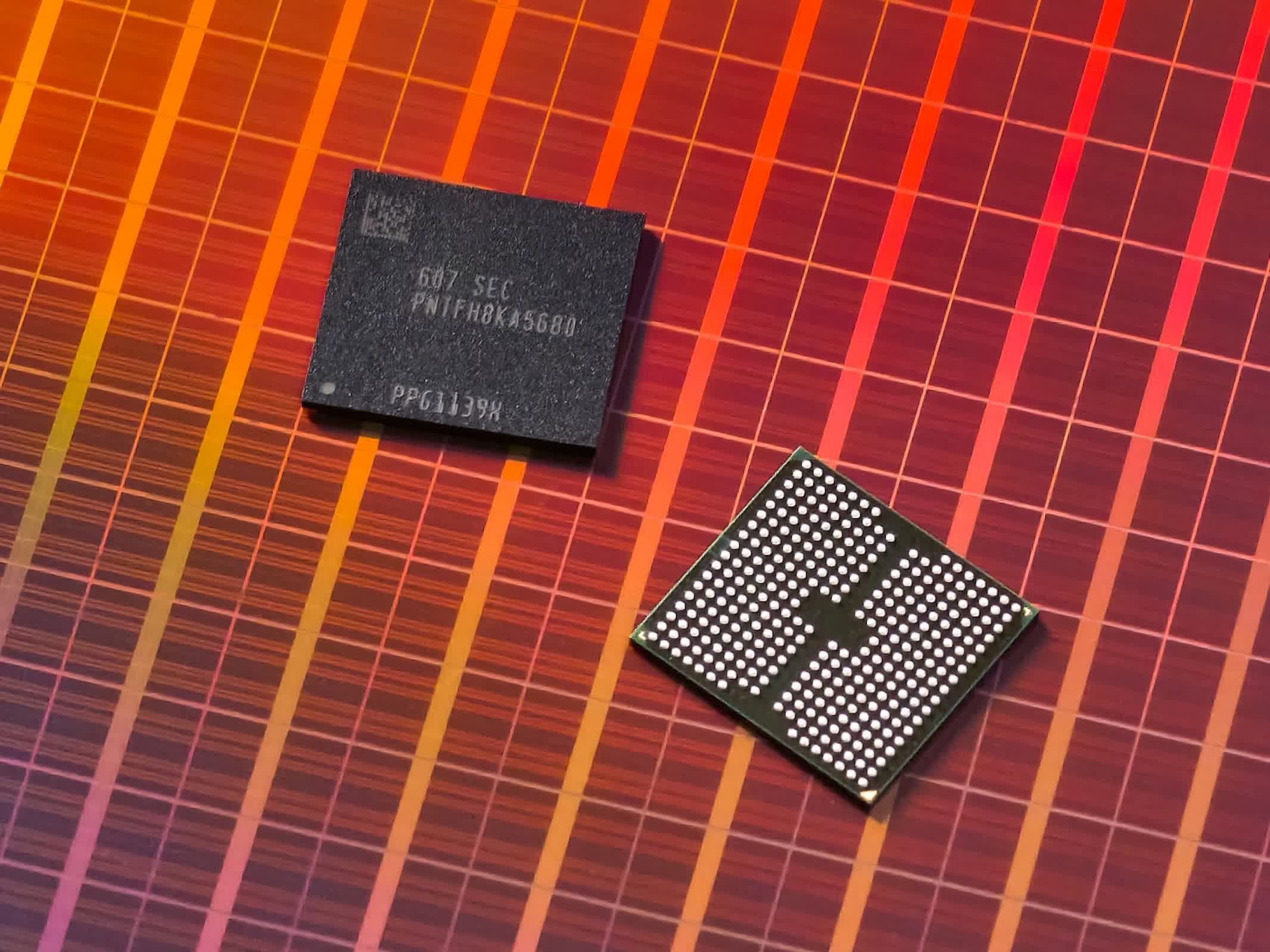
The most concrete product announcement at the show was V10 BV-NAND, which Samsung presented as the industry's first Bonding V-NAND architecture. The device uses wafer bonding to stack memory cells and achieve more than 400 layers in a single chip.
The higher layer count is designed to increase storage density and performance while reducing power consumption. Samsung said V10 BV-NAND boosts memory density by about 58% compared with its V9 generation. It also improves read, write, and input/output performance over V9, targeting high-performance, high-capacity NAND for future AI systems and applications.