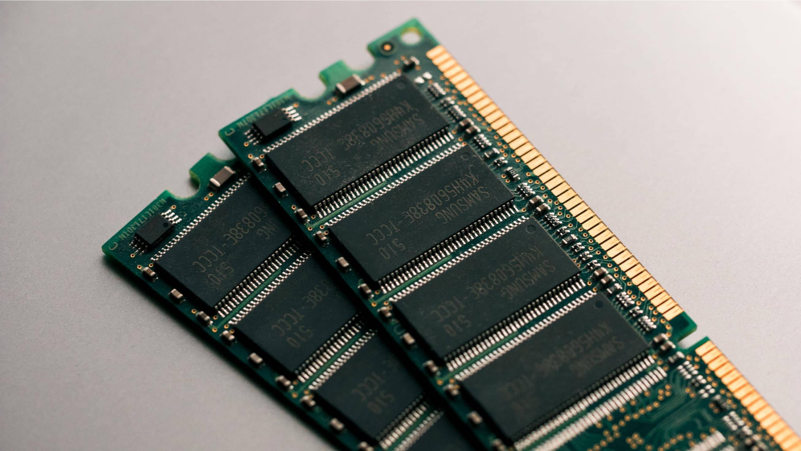
Every single computer has RAM, whether it's embedded into a processor or sitting on a dedicated circuit board plugged into the system, computing devices simply can't work without it. RAM is an astonishing feat of precision engineering, and yet it is manufactured in epic quantities every year. You can count billions of transistors in it, but RAM only uses a handful watts of power. Given how super important RAM is, a proper dissection is called for.
RAM is an astonishing feat of precision engineering, and yet it is manufactured in epic quantities every year.
So let's prep for surgery, wheel out the delivery table, and head for theatre. Time to dig right down into the very cells that make up today's memory and see how it all works.
Wherefore art thou, RAM-eo?
Processors need to be able to access data and instructions very quickly, so they can keep software zipping along. They also need to do this in a way that if it's randomly or unexpectedly requested, the performance isn't affected too much. This is why RAM – short for random-access memory – is really important in a computer.
There are two main types of RAM: static and dynamic, or SRAM and DRAM for short.
We'll be focusing on DRAM, as SRAM is only used inside processors, like a CPU or GPU. So where can we find DRAM in our PCs, and how does it work?
Most people know of RAM because there is a big pile of it right next to the CPU. This group of DRAM often goes by the name of system memory, but a better name would be CPU memory, as it's the main storage for working data and instructions for the processor.
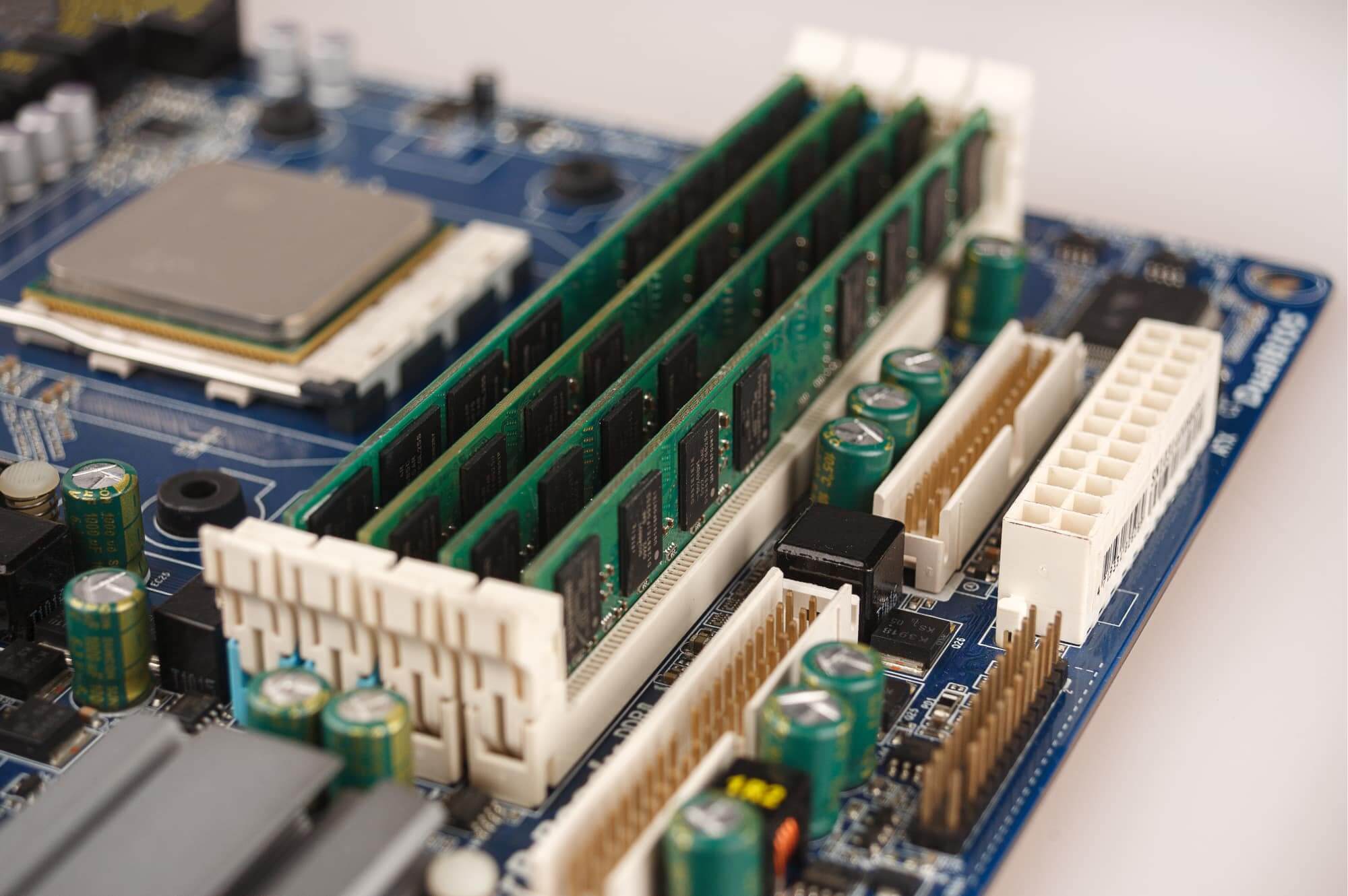
As you can see in the image above, the DRAM sits on small circuit boards that plug into the motherboard. Each board is generally called a DIMM or UDIMM, which stands for dual inline memory module (the U being unbuffered). We'll explain what that means later on, but for now this is the most obvious RAM in any PC.
It doesn't need to be ultra fast, but modern PCs need lots of memory space to cope with big applications and handle the hundreds of processes that run in the background.
The next area to sport a collection of memory chips is usually the graphics card. It needs its own super fast DRAM, because 3D rendering results in a huge amount of data accesses and writes. This kind of DRAM is designed to work in a slightly different way to the type used in system memory.
Here we can see the GPU surrounded by 12 small slabs – these are the DRAM chips. Specifically, they're a type of memory called GDDR5X, which we'll dig into later.
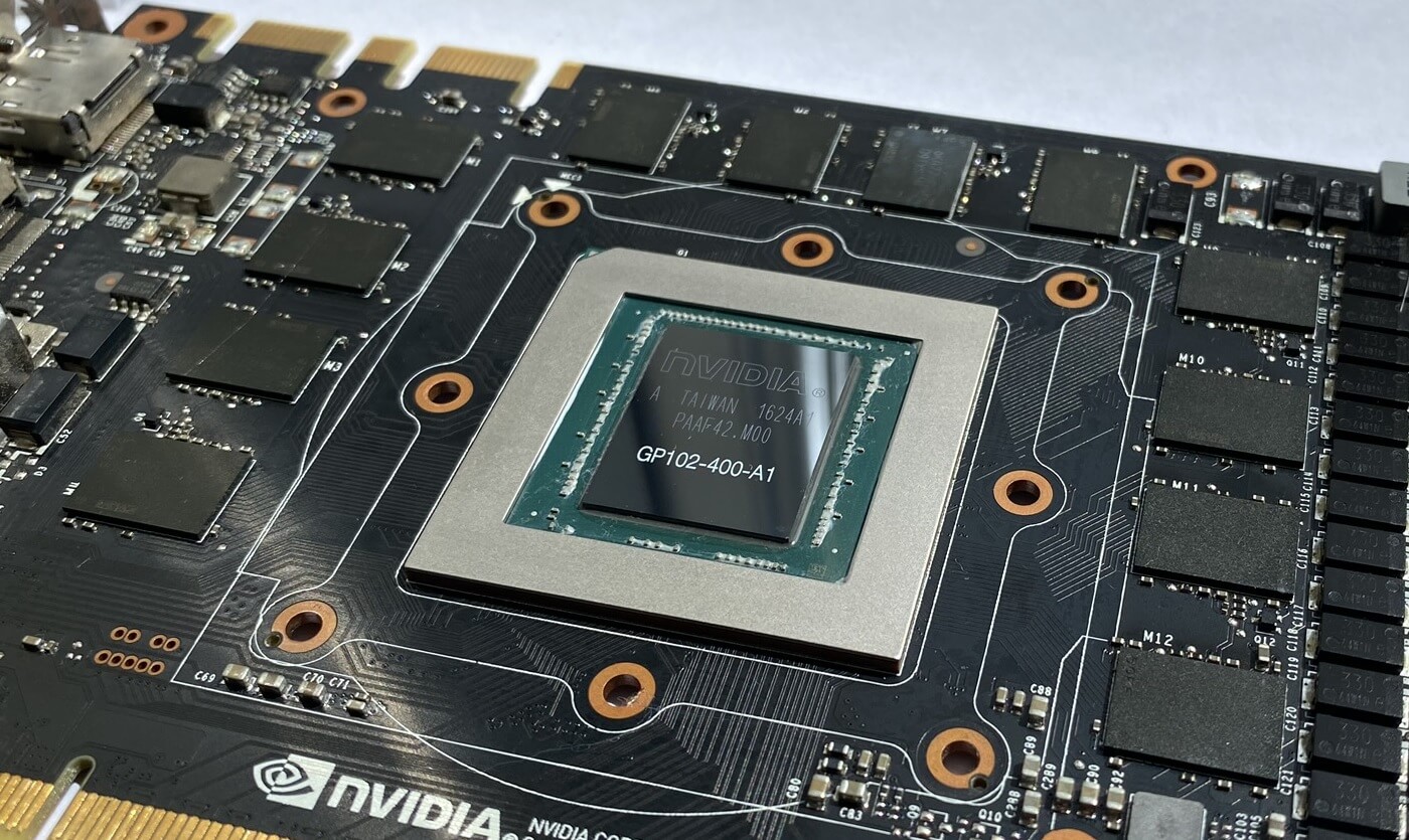
Graphics cards don't need as much memory as the CPU, but it's still thousands of MB in size.
Not every device in a computer require this much: hard drives need a small amount of RAM, 256 MB on average, to group data together before writing it to the drive.
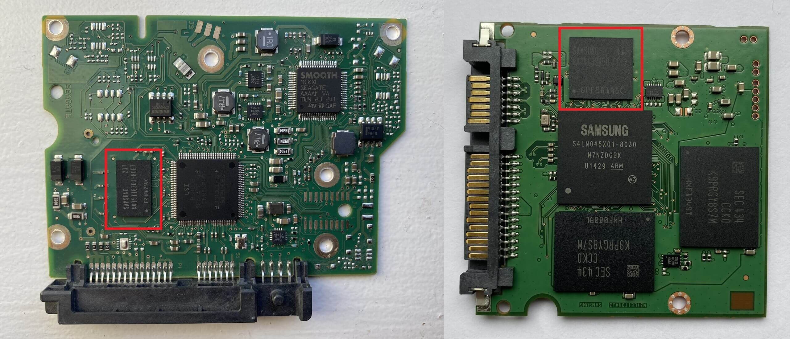
In these images, we can see the circuit board from a HDD (left) and an SSD (right), where the DRAM chip has been highlighted in both examples. Note that it's just the one chip? 256 MB isn't much RAM these days, so a single chunk of silicon is all that is needed.
Once you realize that any component or peripheral which does processing needs RAM, you will soon spot it dotted about the insides of any PC. SATA and PCI Express controllers sport little DRAM chips; network interface and sound cards have it, too, as do printers and scanners.
It seems a bit boring when you see it everywhere, but once you delve into the inner workings of RAM, it's definitely not a yawn fest!
Scalpel. Swab. Electron microscope.
We don't have access to the kind of tools that electronic engineers use to dig deep into their semiconductor creations, so we can't pull apart an actual DRAM chip and show you the insides. However, the folks over at TechInsights do have such equipment and produced this image of the chip surface:
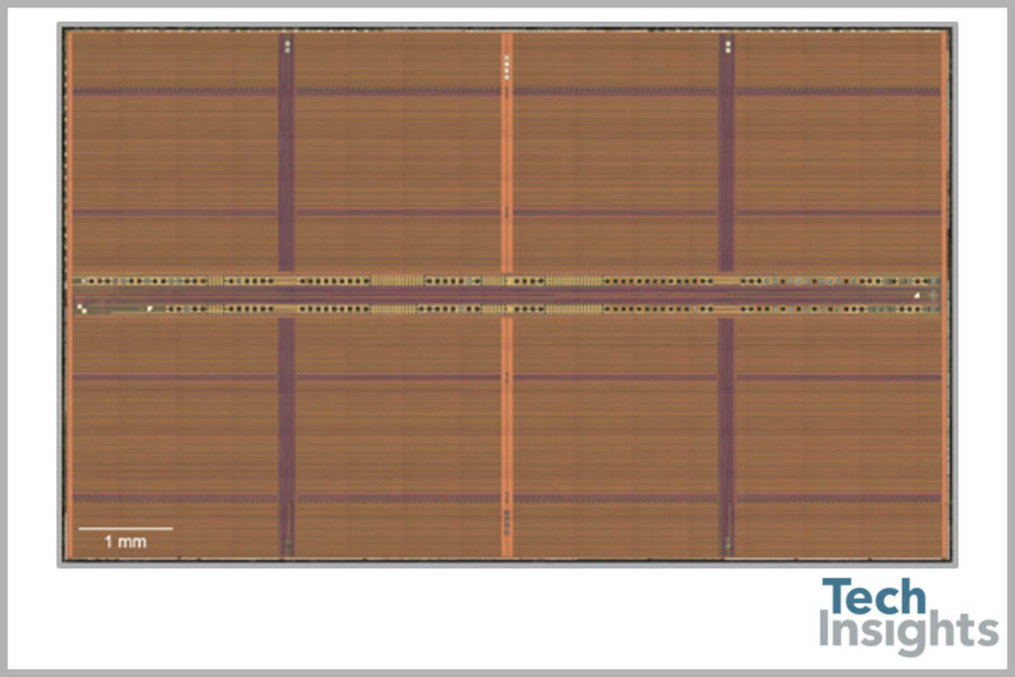
If you're thinking that this just looks like crop fields connected by pathed roads, then you're not far off the mark as to what's actually there! Instead of corn or wheat, the fields in a DRAM are mostly made up two electronic components:
- A switch, in the form of a MOSFET (metal oxide semiconductor field-effect transistor)
- Some storage, handled by a trench capacitor
Together, they form what is called a memory cell and each one stores 1 bit of data. A very rough circuit diagram for the cell is shown below (apologies to all electronic engineers!):
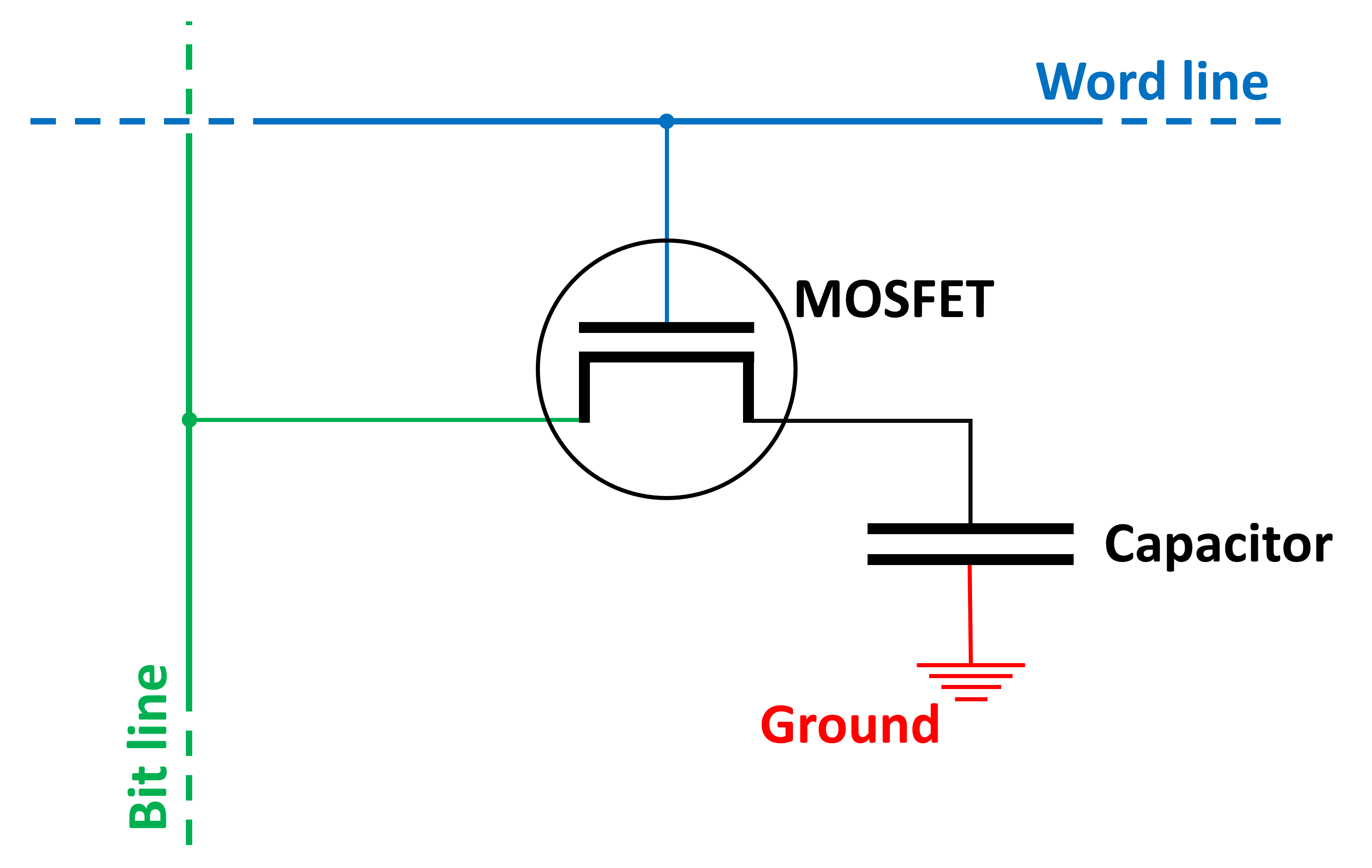
The blue and green lines represent connections that apply a voltage to the MOSFET and capacitor. These are used to read and write data to the cell, and the vertical one (the bit line) is always fired up first.
The trench capacitor basically acts as a bucket, filling up with electrical charge – its empty/full state gives you that 1 bit of data: 0 for empty, 1 for full. Despite the best efforts of engineers, the capacitors can't hold onto this charge forever and it leaks away over time.
This means that every single memory cell needs to be regularly refreshed, between 15 and 30 times a second, although the process itself is pretty quick: just a few nanoseconds is needed for a collection of cells. Unfortunately, there are lots of cells in a DRAM chip and the memory can't be read or written to while it's being charged back up.
Multiple cells are connected to each line, as shown below.
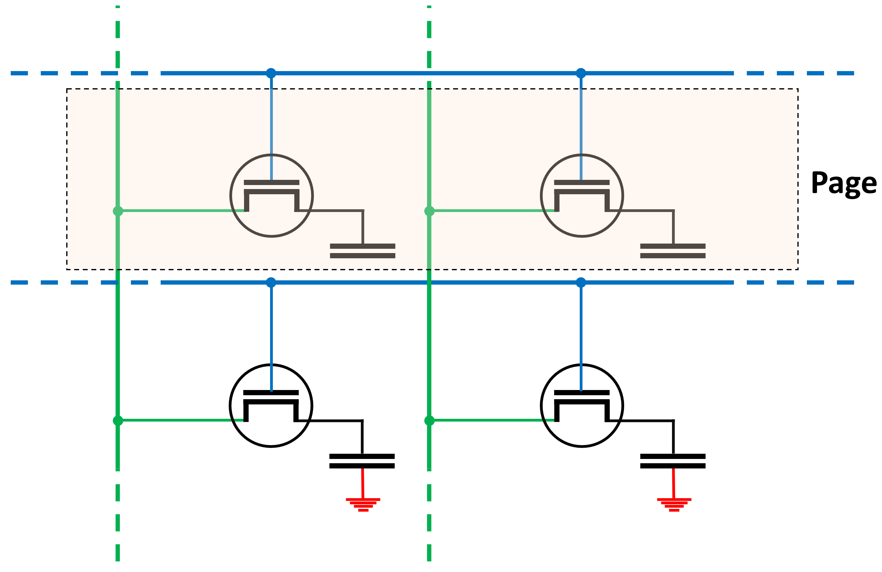
A full row of memory cells is called a page and the length of it varies between DRAM types and configurations. A longer page will have more bits, but more electrical power is required to operate it; shorter pages use less power, but there's less storage.
However, there is another important factor that needs to be considered. When reading or writing from/to a DRAM chip, the first step in the process is to activate an entire page. The row of bits (a string of 0s and 1s) are stored in a row buffer, which is actually a collection of amplifiers and latches, rather than more memory. Then the required column is activated, to pull the relevant data out of this buffer.
If the page is too small, then the rows have to be activated more frequently to meet the data requests; on the other hand, a large page will essentially cover more bases, so they won't need to be activated as often. Even though a long row needs more power, and potentially be less stable, it's better to have the biggest pages you can get.
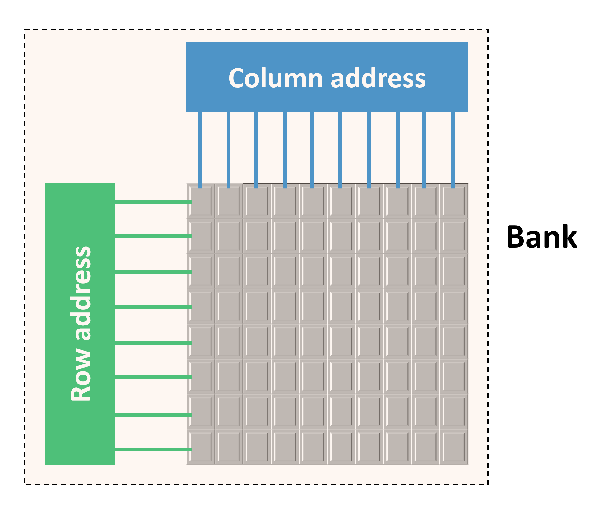
Putting a collection of pages together gives us one bank of DRAM. As with pages, the size and arrangement of the rows and columns of cells plays a big part in how much data can be stored, how fast it can operate, power consumption, and so on.
One such arrangement might consist of 4,096 rows and 4,096 columns, giving one bank a total storage capacity of 16,777,216 bits or 2 MB. But not all DRAM chips have their banks in a 'square' organization as it's better to have longer pages, rather than shorter ones. For example, an organization of 16,384 rows and 1,024 columns would still result in 2 MB of storage, but each page contains 4 times more data than the square example.
All of the pages in a bank are connected to a row address system (likewise for the columns) and these are controlled by command signals and addresses for each row/column. The more rows and columns there are in a bank, the more bits needed to be used in the address.
For a 4,096 x 4,096 bank, each addressing system requires 12 bits, whereas a 16,384 x 1,024 bank would need 14 bits for the row address, and 10 bits for the columns. Note that both systems are a total of 24 bits in size.
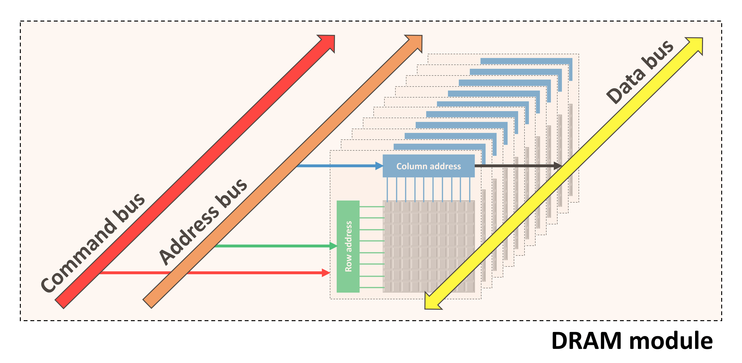
If a DRAM chip only offered up one page at a time, it wouldn't be of much use, so they have several banks of memory cells packed into them. Depending on the overall size, the chip might have 4, 8, or even 16 banks – the most common format is to have 8.
All of the banks share the same command, address, and data buses, which simplifies the overall structure of the memory system. While one bank is busy sorting out one instruction, different banks can still be carrying out other operations.
The entire chip, containing the banks and buses, are packaged into a protective shell and then soldered onto a circuit board. This contains electrical traces which provides the power to operate the DRAM and the signals for the commands, addresses, and data.
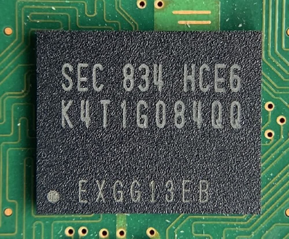
In the above image, we can see a DRAM chip (sometimes called a module) made by Samsung – other top manufacturers include Toshiba, Micron, SK Hynix, and Nanya. Samsung is the largest producer, having roughly 40% of the global market share.
Each DRAM producer use their own coding system to identify the memory specifications, but the above example is a 1 Gbit chip, fielding 8 banks of 128 Mbits, arranged in 16,384 rows and 8,192 columns.
Name and rank, soldier!
Memory companies take several DRAM chips and put them together on a single circuit board, called a DIMM. Although the D stands for dual, it doesn't mean there are two sets of chips – rather, it refers to the electrical contacts along the bottom of the board, with both sides used for handling the modules.
DIMMs themselves vary in size and the number of chips on them:
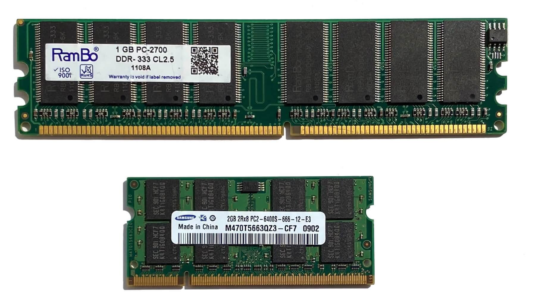
In the above image, we can see a standard desktop PC DIMM, whereas the one underneath is called a SO-DIMM (small outline DIMM). The small module is designed to be used in smaller form factor PCs like a laptop or all-in-one desktop. Packing everything into a smaller space limits how many chips can be used, what speed everything runs at, and so on.
There are three key reasons for using multiple memory chips on the DIMM:
- It increases the amount of storage available
- Only one bank can be accessed at any one time, so having others working in the background improves performance
- The address bus in the processor handling the memory is wider than the DRAM's bus
The latter is really important, because most DRAM chips only have an 8-bit data bus. CPUs and GPUs, though, are quite a bit different: AMD's Ryzen 7 3800X CPU has two 64-bit controllers built into it, whereas their Radeon RX 5700 XT packs eight 32-bit controllers into it.
So each DIMM that gets installed into the Ryzen computer will need to have eight DRAM modules (8 chips x 8 bits = 64 bits). You might think that the 5700 XT graphics card will have 32 memory chips, but it only has 8. So what gives?
Memory chips designed for use in graphics scenarios pack more banks into the chip, usually 16 or 32, because 3D rendering needs to access lots of data at the same time.

The set of memory modules that "fill" the memory controller's data bus is called a rank and although it's possible to have more than one rank wired to a controller, it can only pull data off one rank at any one time (as they're all using the same data bus). This isn't a problem, because while one rank is busy responding to a given instruction, a new set of commands can be fired off to another rank.
DIMMs can actually have more than one rank on them and this is especially useful if you need a massive amount of memory, but you've only got a relatively small numbers of RAM slots on the motherboard.
So-called dual or quad ranked setups can potentially offer more overall performance than single ranked ones, but piling on the ranks causes the load on the electrical system to rapidly build up. The majority of desktop PCs will only handle one or two ranks for each controller. If a system needs to have a lot more than this then it's best to use buffered DIMMs: these have an extra chip on the DIMM that eases the load on the system by storing instructions and data for a few cycles before sending it onwards.
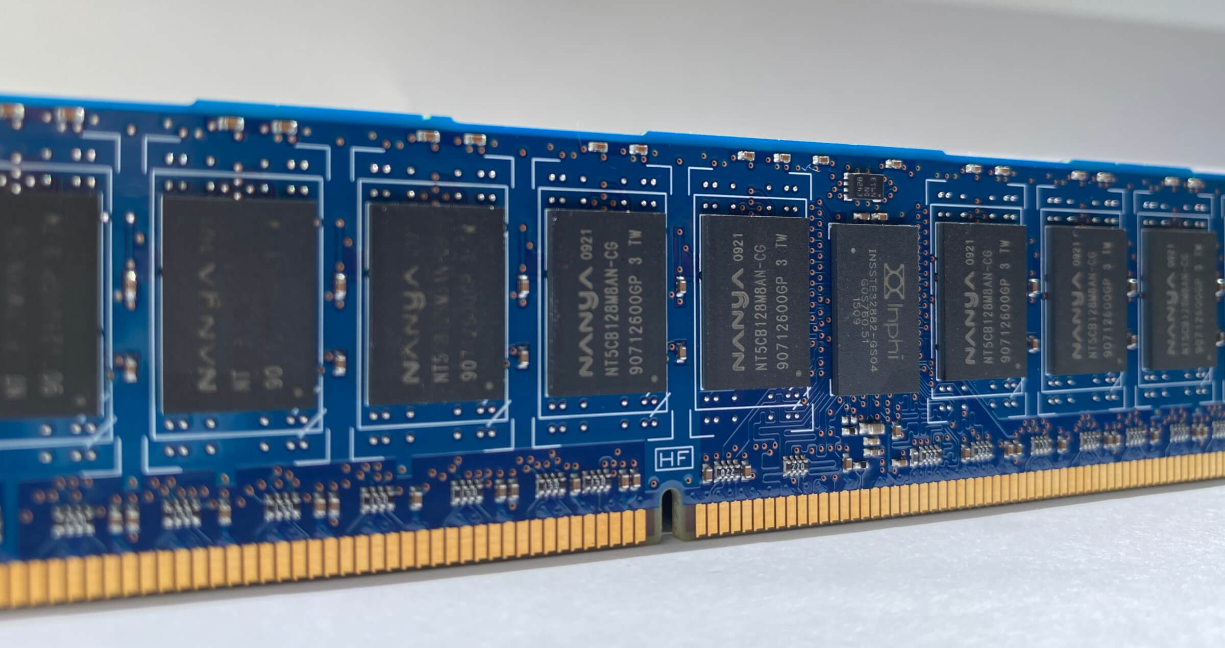
Not all ranks are 64 bits in size, either – DIMMs used in servers and workstations are often 72 bits, which means they have an extra DRAM module on them. The extra chip doesn't give more storage or performance; instead, it's used for error checking and correcting (ECC).
Remember that all processors need memory to work? Well, in the case of ECC RAM, the little device that does the work is given its own module.
The data bus in such memory is still only 64 bits wide, but the reliability of the data is improved considerably. The use of buffers and ECC only knocks a little bit of the overall performance, but adds quite a bit to the cost.
I feel the need – the need for speed!
All DRAM has a central I/O clock (input/output), a voltage that constantly changes between 2 levels, and this is used to organize everything that takes places in the memory chip and buses.
If we go back in time to 1993, you would have been able to buy memory in the form of SDRAM (synchronous DRAM), which sequenced all processes using the period of time when the clock is changing from the low to high state. Since this happens very quickly, it provides a very accurate way of indicating when events must occur. SDRAM back then had I/O clocks that typically ran from 66 to 133 MHz, and for every tick of the clock, one instruction could be issued to the DRAM. In return, the chip could transfer 8 bits of data in the same amount of time.
The rapid development of SDRAM, lead by Samsung, saw a new form of it appear in 1998. It timed data transfers on the rise and fall of the clock voltage, so for every tick of that clock, data could be send to and from the DRAM twice.
The name for this exciting new technology? Double data rate synchronous dynamic random access memory. You can see why everyone just called it DDR-SDRAM or DDR for short.
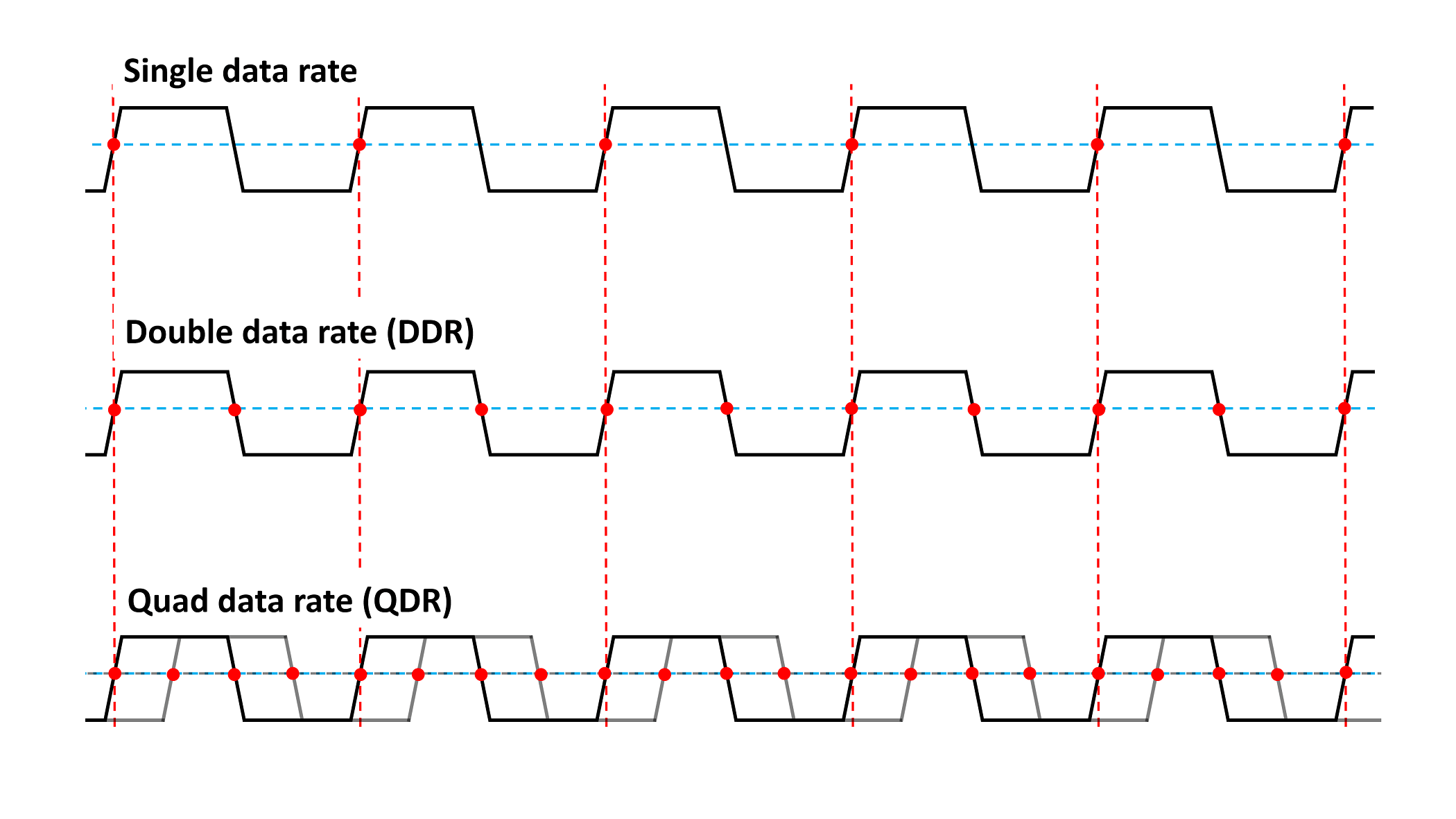
DDR memory rapidly became the norm (causing the original SDRAM to be renamed as single data rate SDRAM, SDR-DRAM) and has been the mainstay for all computer systems for 20 years.
Advances in technology helped improve the technology, giving us DDR2 in 2003, DDR3 in 2007, and DDR4 by 2012. Each update provided better performance thanks to faster I/O clocks, better signalling systems, and lower power requirements.
DDR2 started a change that's still in use today: the I/O clock became a separate system that timed itself from another set of clocks in such a way that it's now 2 times faster. It's a similar principle to how CPUs use a 100 MHz clock to sequence everything but the processor's internal clocks run 30 or 40 times faster.
DDR3 and 4 upped the game by having the I/O clock run 4 times, but in all cases the data bus still only uses the rise and fall of the I/O clock (i.e. double data rate) to send/receive information.
The memory chips themselves aren't running at stupidly high speeds – in fact, they chug along relatively slowly. The data transfer rate (measured in millions of transfers per second, MT/s) in modern DRAM is so high, because of the use of multiple banks in each chip; if there was only one bank per module, everything would be desperately slow.
| DRAM type | Typical chip clock | I/O clock | Data transfer rate |
| SDR | 100 MHz | 100 MHz | 100 MT/s |
| DDR | 100 MHz | 100 MHz | 200 MT/s |
| DDR2 | 200 MHz | 400 MHz | 800 MT/s |
| DDR3 | 200 MHz | 800 MHz | 1600 MT/s |
| DDR4 | 400 MHz | 1600 MHz | 3200 MT/s |
Each DRAM revision retains no backwards compatibility, so the DIMMs used for each type has different amounts of electrical contacts, slots and notches, to prevent anyone from trying to jam DDR4 memory into a DDR-SDRAM slot.
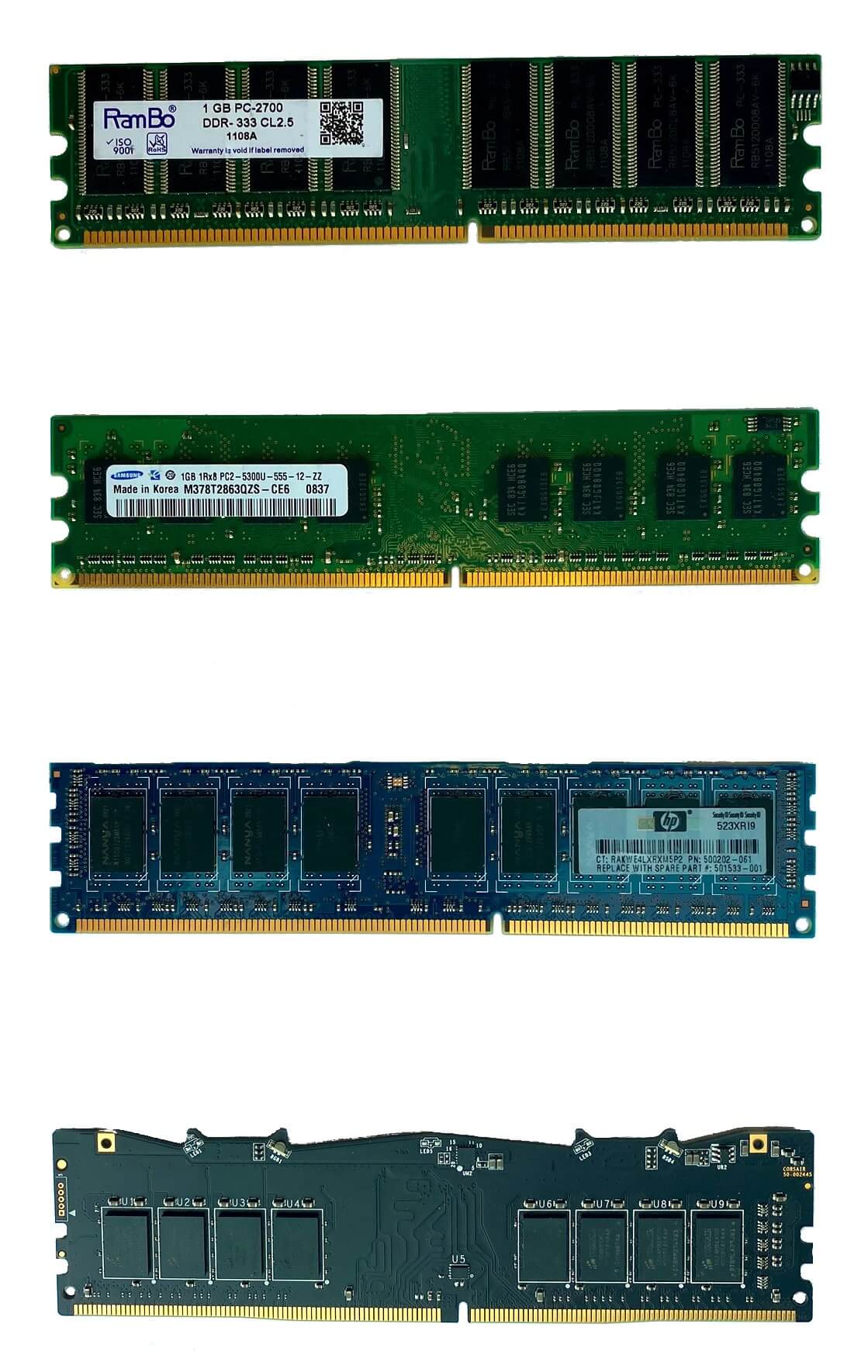
DRAM for graphics applications was originally called SGRAM or synchronous graphics RAM. That type of RAM has also gone through the same kind of development, and today is labelled GDDR to make it's intended use clearer. We're now on version 6 and data transfers use a quad data rate system, i.e. 4 transfers per clock cycle.
| DRAM type | Typical chip clock | I/O clock | Data transfer rate |
| GDDR | 250 MHz | 250 MHz | 500 MT/s |
| GDDR2 | 500 MHz | 500 MHz | 1000 MT/s |
| GDDR3 | 800 MHz | 1600 MHz | 3200 MT/s |
| GDDR4 | 1000 MHz | 2000 MHz | 4000 MT/s |
| GDDR5 | 1500 MHz | 3000 MHz | 6000 MT/s |
| GDDR5X | 1250 MHz | 2500 MHz | 10000 MT/s |
| GDDR6 | 1750 MHz | 3500 MHz | 14000 MT/s |
Besides faster rates, graphics DRAM offers extra features to help the flow of rates such as being able to open up two pages at the same time in a bank, command and address buses running at DDR, or the memory chips running at much higher clock speeds.
The downside to all this advanced technology? Cost and heat.
One module of GDDR6 is roughly twice the price of an equivalent DDR4 chip and gets pretty toasty when running at full speed – this is why graphics cards sporting large amount of super fast RAM need active cooling to stop the chips from overheating.
Hickory Dickory Dock
DRAM performance is usually rated by the number of bits of data it can transfer per second. Earlier in this article, we saw that DDR4 used as system memory has 8 bit wide chips – these means that each module can transfer up to 8 bits per clock cycle.
So if the data transfer rate is 3200 MT/s, this would result in a peak of 3200 x 8 = 25,600 Mbits per second or a little over 3 GB/sec. Since most DIMMs have 8 chips on them, that gives a potential 25 GB/sec. For the likes of GDDR6, 8 modules of that would be nearly 440 GB/sec!
Most people call this value the bandwidth of the memory and it's an important factor behind performance of RAM. However, this is a theoretical figure because everything inside the DRAM chip doesn't take place at the same time.
To understand this, take a look at the image below. It's a very simplified (and unrealistic) overview of what happens when data is requested from the memory.
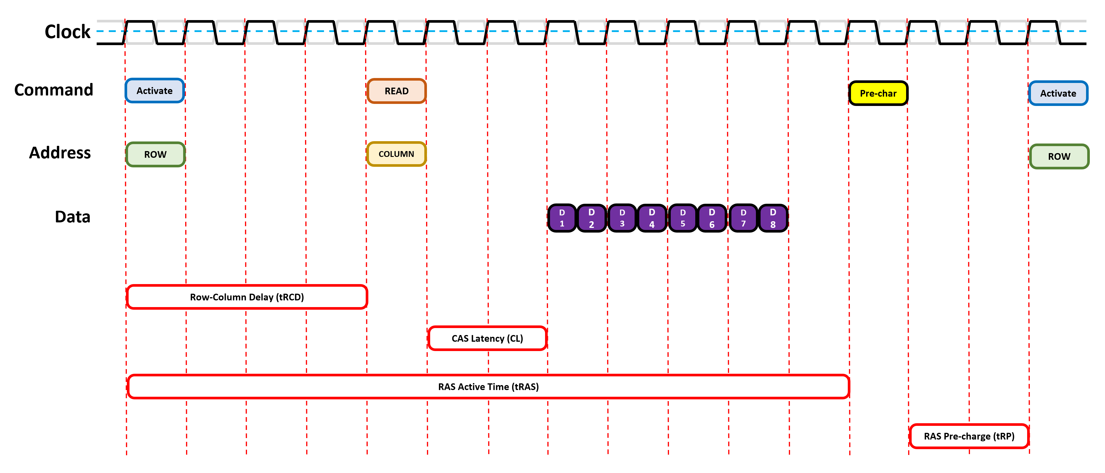
The first stage involves activating the page in the DRAM that holds the required data. This is done by first telling the memory which rank is needed, then the relevant module, followed by the specific bank.
The location of the page in all of that (the row address) is issued to the chip and it responds by firing up that entire page. It takes time to do all of this and, more importantly, enough time needs to be given for the row to fully activate – this is to ensure that the whole row of bits is locked down, before it can be accessed.
Then the relevant column is identified, pulling out the single bit of information. All DRAM sends data in bursts, packing the information into a single block, and the size of the burst in today's memory is nearly always 8 bits. So even if the single bit from one column is retrieved in a single clock cycle, that data can't be sent off until the other 7 bits are pulled down from other banks.
And if the next bit of data required is on another page, the one currently open needs to be shut down (the process is called pre-charging) before the next one can be activated. All of which, of course, takes more time.
All these different periods, between when an instruction has been sent and the required action has taken place, are called memory timings or latencies. The lower the value, the better the overall performance, simply because you're spending less time waiting for something to happen.
Some of these latencies will have familiar names to PC enthusiasts:
| Timing name | Description | Typical value in DDR4 |
| tRCD | Row-to-Column Delay: the number of cycles between a row being activated and then the column being selectable | 17 cycles |
| CL | CAS Latency: how many cycles between a column being address and the data burst starting | 15 cycles |
| tRAS | Row Cycle Time: the shortest number of cycles a row must stay active before it can be pre-charged | 35 cycles |
| tRP | Row Precharge time: the minimum of cycles needed between different row activations | 17 cycles |
There are lots of other timings and they all need to be carefully set to ensure the DRAM operates in a stable manner, without corrupting data, at the best possible performance. As you can see from the table, the diagram showing the cycles in action needs to be a lot wider!
Although there is a lot of waiting involved, instructions can be queued and issued, even if the memory is busy doing something. This is why we see lots of RAM modules where we need the performance (system memory for the CPU and on graphics cards), and then just the one where it's far less important (in hard drives).
Memory timings are adjustable – they're not hard-wired into the DRAM itself, because all instructions come from the memory controller in the processor using the RAM. Manufacturers test every chip they make and those that meet certain speed ratings, for a given set of timings, are grouped together and installed on DIMMs. The timings are then stored on a little chip that's fitted to the circuit board.

The process for accessing and using this information is called serial presence detect (SPD). It's an industry standard for letting the motherboard BIOS know what timings everything needs to be set to.
Lots of motherboards allow you to alter these timings yourself, either to improve performance or raise the stability of the platform, but many DRAM modules also support Intel's Extreme Memory Profile (XMP) standard. This is nothing more than extra information stored in the SPD memory that says to the BIOS, 'I can run with these non-standard timings.' So rather than messing about with the settings yourself, a simple click and the job is done for you.
Wham, bam, thank you RAM!
Unlike our other anatomy lessons, this one wasn't so messy – there's very little to take apart with DIMMs and specialized tools are needed for the modules. But that lack of guts and gibbets hides some amazing details.
Take an 8 GB DDR4-SDRAM memory stick from any new PC and you'll be holding something that's packing nearly 70 billion capacitors and the same number again for transistors. Each one storing a scant amount of electrical charge, and being accessed in just a handful of nanoseconds.
It will run through a countless number of instructions, even in normal daily use, and most can do this for years on end, before suffering any problems. And all this for less than $30? That's nothing short of mind-blowing!
DRAM continues to improve – DDR5 is just around the corner and promises the level of bandwidth per module that two full DIMMs of DDR4 will struggle to reach. It'll be very expensive when it does appear, but for servers and professional workstations, the leap in performance will be very welcome.
As always, if you've got any questions about RAM in general or you've got some cool tips about tweaking the memory timings, send them our way in the comments section below. Stay tuned for even more anatomy series features.
Article image credit: Harrison Broadbent (masthead), daniiD (RAM next to CPU)
