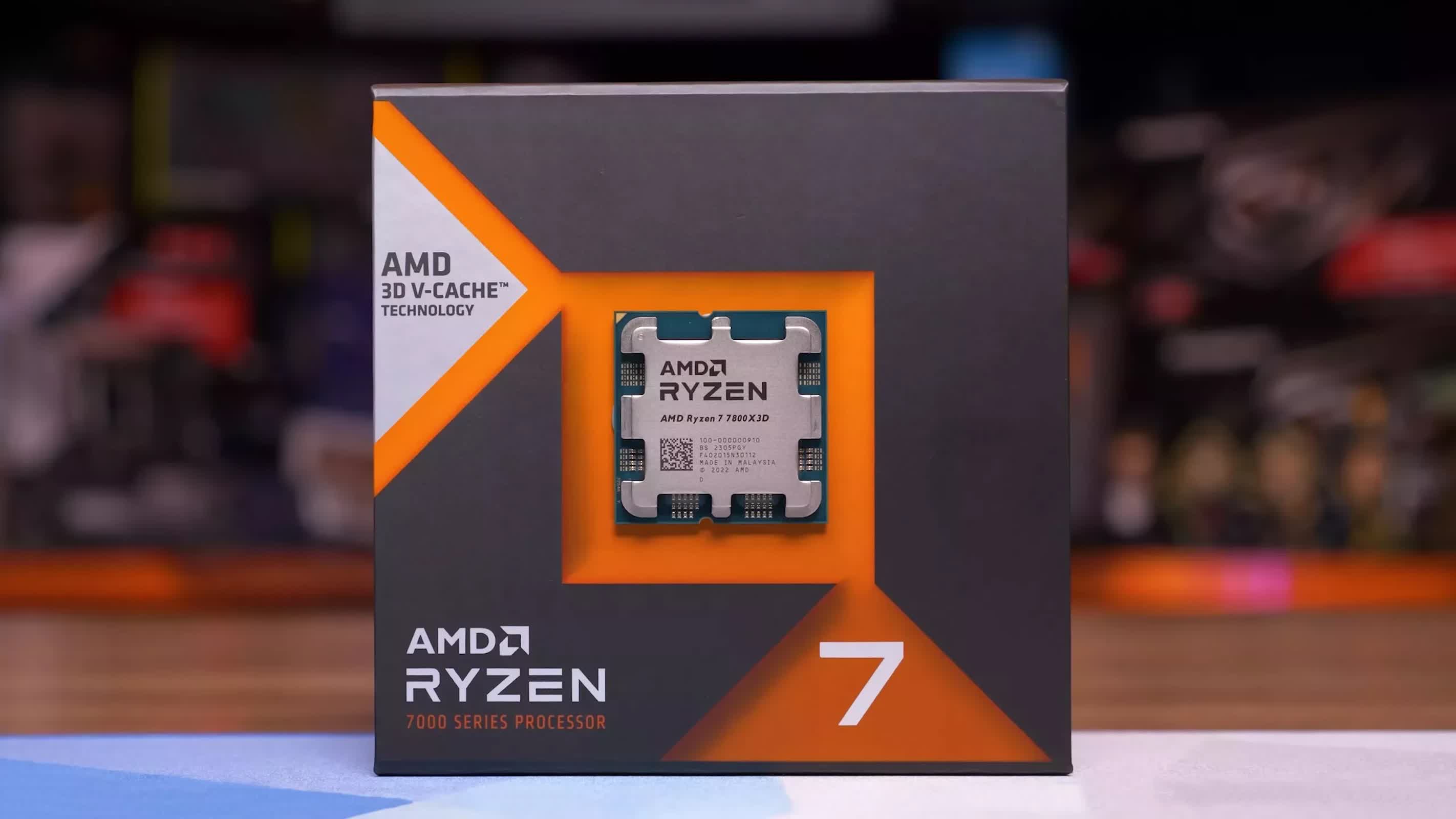
What we know so far: AMD's new Instinct MI450 is a statement of intent. Built on the cutting-edge 2nm process and backed by a major partnership with OpenAI, the accelerator signals a turning point in how AI hardware is designed and scaled. The move puts fresh pressure on Nvidia and others to rethink their roadmaps, as the race to power ever-larger AI models pushes the limits of what silicon, and the industry, can deliver.
AMD is staking its claim as a technological leader in AI hardware, confirming that its forthcoming MI450 accelerator will use an advanced 2-nanometer fabrication process – a significant leap ahead of rival Nvidia, whose next-generation Vera Rubin GPUs are expected to be built on a 3-nanometer node. The announcement came amid growing industry competition for powering increasingly complex artificial intelligence workloads.
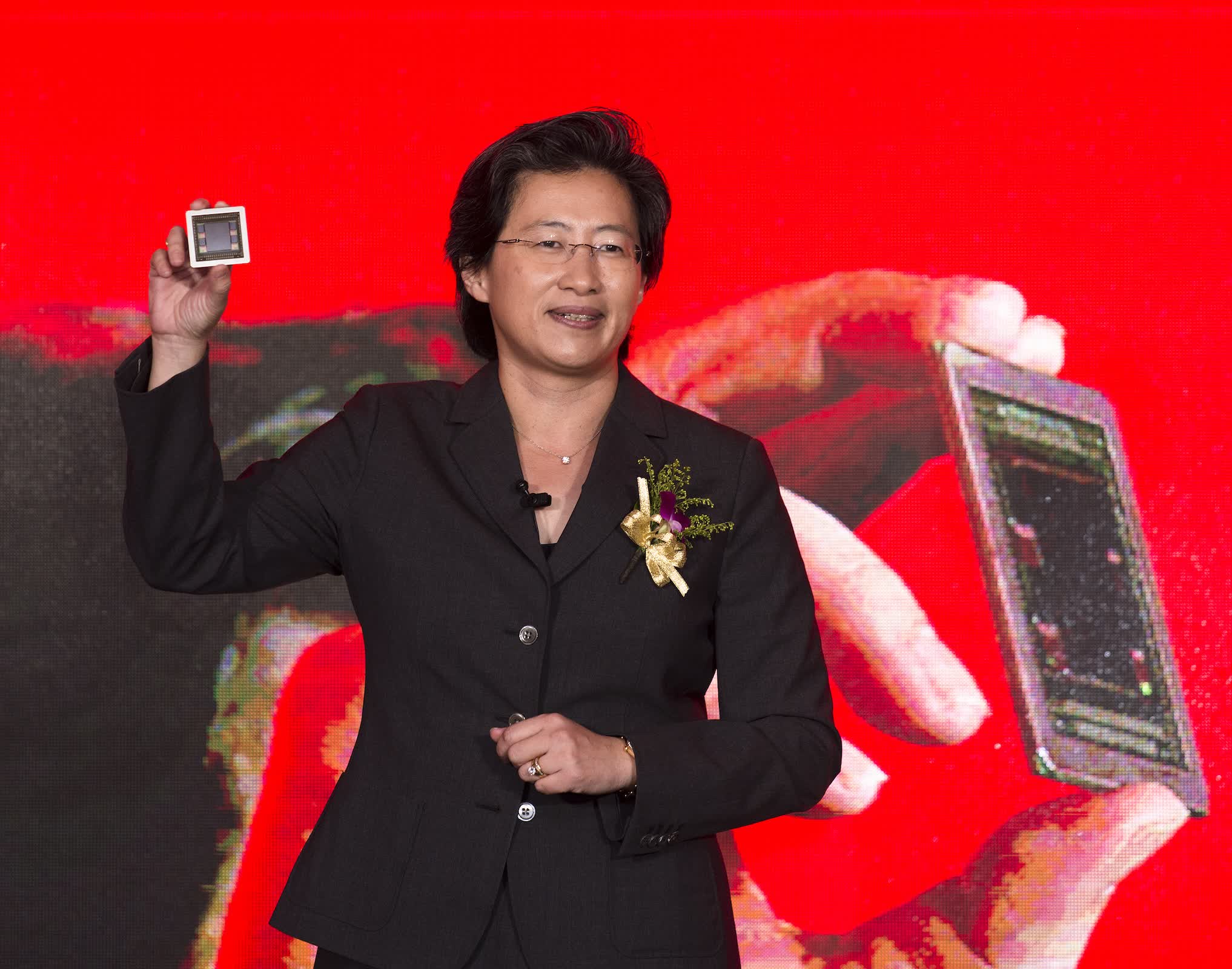
In a recent interview with Yahoo Finance following a high-profile partnership with OpenAI, AMD Chief Executive Lisa Su confirmed the 2nm milestone. According to Su, the MI450 accelerator, scheduled to be released in 2026, will incorporate the latest TSMC fabrication technology for its core computational die – a decision expected to deliver advancements in thermal efficiency and computing power.
The 2nm process will be used exclusively for the MI450's Accelerator Core Die (XCD). Other components, including the Active Interposer Die (AID) and Media Interface Die (MID), will utilize TSMC's refined 3nm node, reflecting a hybrid approach to optimizing each segment of the GPU design for its specific computational role. This layered architecture combines ultra-dense, high-speed cores with robust interconnect and media handling subsystems, aiming to address AI workloads that demand massive parallel processing and efficient data movement at scale.
Su detailed the magnitude of AMD's collaboration with OpenAI, describing a "six gigawatt" deployment that is expected to generate tens of billions of dollars in revenue over the next several years. According to the CEO, the deal will make OpenAI a lead customer for the MI450 generation.
The scope of the initiative highlights the scale of AI infrastructure development underway globally. Su described the challenge of building out a multi-gigawatt computing backbone for the "next era" of artificial intelligence. She acknowledged that building millions of high-performance GPUs – each engineered with advanced silicon and supported by rack-scale integration – is an immense technical feat, touching everything from manufacturing capacity to energy infrastructure.
Su also addressed broader industry concerns about potential risks or bottlenecks, noting that collaboration across the ecosystem, from chipmakers and cloud providers to government and enterprise, will be essential for scaling AI deployments. "This is one of those points in time where you need every part of the food chain to come together and say, 'we want to do this, we want to build fast, we want to build big,'" said Su.
AMD taps TSMC's 2nm node to challenge Nvidia in next-gen AI compute
