Intel's 18A found to be faster but TSMC's N2 is denser in process node showdown

zohaibahd

Posts: 976   +19
Staff
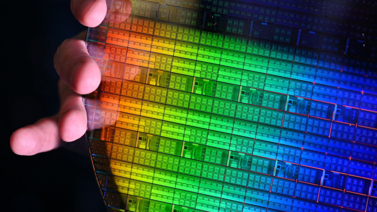
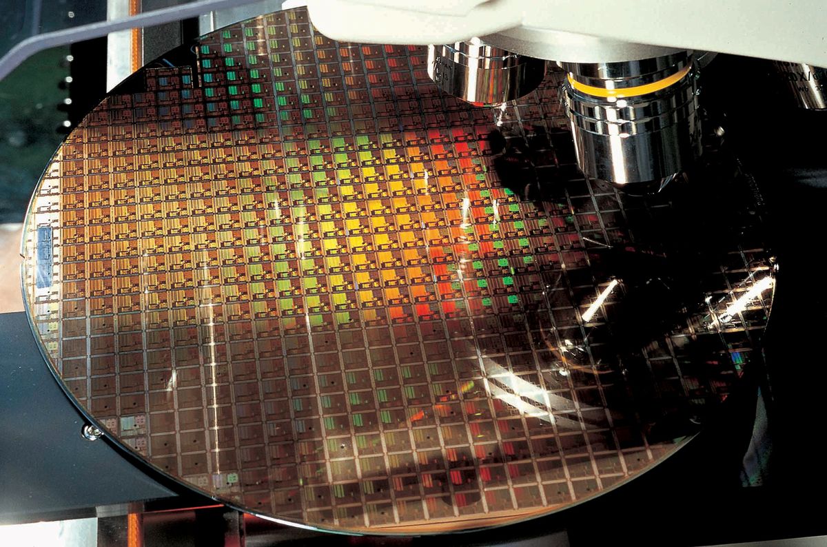
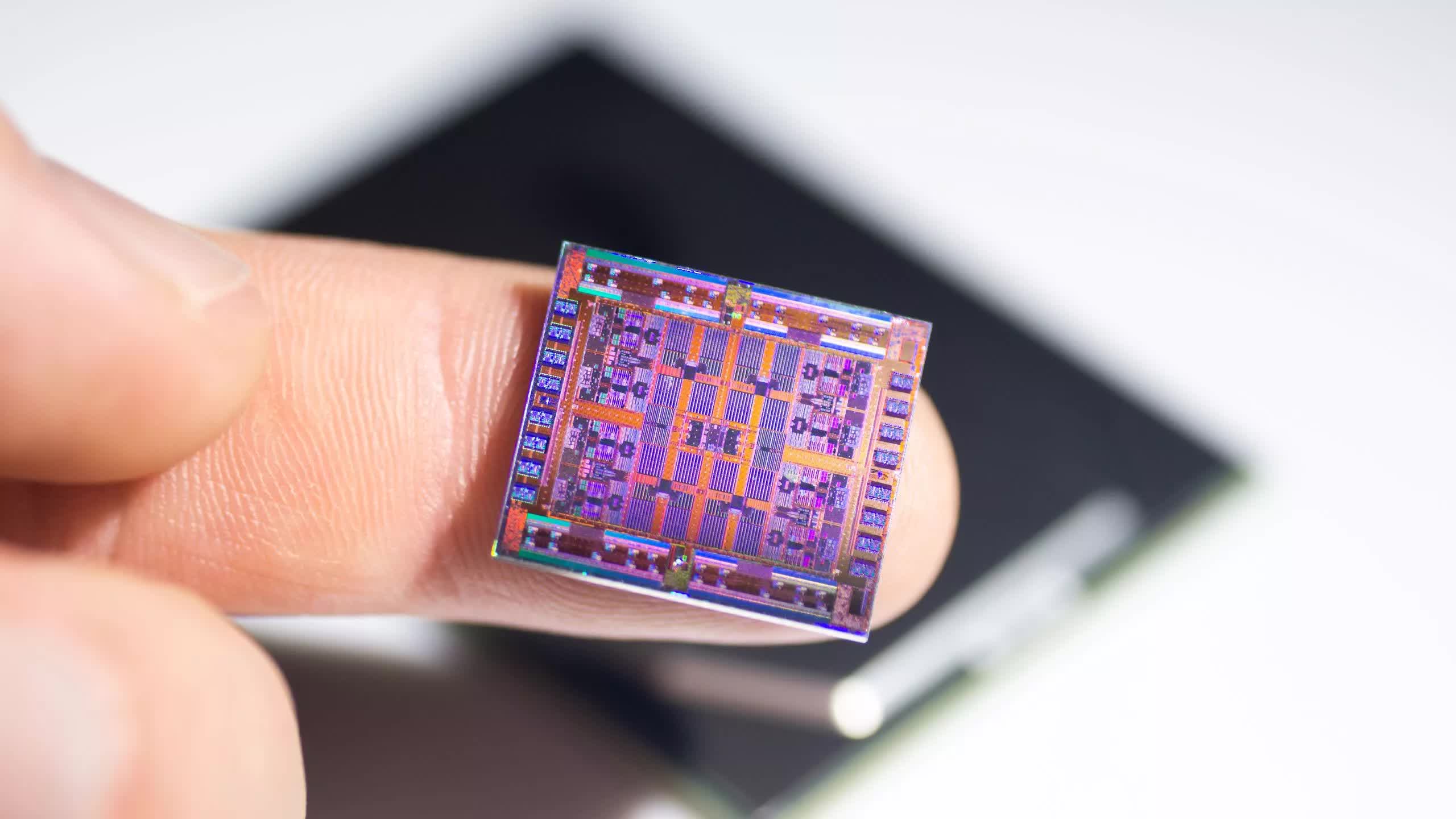
Bottom line: Intel and TSMC are both gearing up to launch their respective 18A and N2 process nodes, each offering significant advancements. On one side, Intel claims 18A will deliver much higher generational performance gains. On the other, TSMC is emphasizing N2's impressive transistor density. But which one is truly superior? As it turns out, the answer isn't so straightforward.

A new report from TechInsights breaks things down, suggesting we could be in for a closely matched competition.

When it comes to transistor density, TSMC's N2 appears to take the lead. The publication's data estimates N2's high-density standard cell transistor density at an impressive 313 million transistors per square millimeter, outpacing Intel's 18A at 238 million and Samsung's SF3 at 231 million. Of course, density isn't everything; chip designers use a mix of high-, standard-, and low-power cells. However, TSMC's advantage in density could provide an edge for certain workloads.

The comparison becomes less clear when it comes to performance projections. Intel's 18A may have an advantage over TSMC's N2 and Samsung's SF3, but these are still just estimates based on extrapolating from previous node improvements.

What we do know is that Intel is equipping 18A with its new PowerVia backside power delivery technology to enhance speed and efficiency. While TSMC has plans for a similar approach in the future, N2 won't include it. However, it's worth noting that not every 18A chip will feature this technology.

When it comes to efficiency, analysts expect N2 chips to outperform 18A and Samsung's offerings. TSMC has consistently led in power efficiency, so this projection aligns with recent trends.

Another key differentiator is production timelines. Intel remains ahead, with 18A set to enter high-volume manufacturing for next-gen Core Ultra processors by mid-2025. These chips are expected to hit shelves before the end of the year. Meanwhile, TSMC's N2 volume production won't begin until late 2025, meaning the first N2-based products likely won't arrive until mid-2026 at the earliest, following standard industry timelines.

In summary, TSMC holds the transistor density lead with N2, but Intel's 18A could take the performance crown thanks to architectural advancements and innovations like PowerVia. Additionally, Intel's head start in production means 18A silicon will be available in real-world products much sooner.

Permalink to story:

 
Although Intel has done downright illigal things in the past and them being complacent with quad cores when there was no competition got them in the situation they're in... I do hope that they overcome this.
We need the competition, Intel wanting external customers for their fabs could also be interesting if this process results in faster chips. An AMD chip manufactured by Intel would be entertaining.
 
Last edited:
Yes, we'll take random internet guy's word over the experts. All you have to do is yell "fake news" to win the day... but that only works on Orange Twitter, not here.

What exactly are you questioning? Higher density provides more room to drive generational performance in your design. SRAM (caches) is the most complex component to shrink and by far one of the largest part of the chip. Whether you accept it or not, TSMC outperforms Intel in every aspect.

This article plays with words, as Intel is currently at rock bottom.

"Tom’s Hardware has got its paws on an ISSCC 2025 Advance Programme paper which says that Chipzilla’s 18A manufacturing process (1.8nm-class) will have an SRAM density closer to TSMC’s N3 (3nm-class) than its N2 (2nm-class). If this is correct than Intel’s process might not be as competitive.

The report said that Intel’s 18A process has a high-density SRAM bit cell size of 0.021 µm², resulting in an SRAM density of approximately 31.8 Mb/mm². This represents a notable improvement over Intel 4's 0.024 µm² bit cell size but aligns closely with TSMC’s N3E and N5 processes. By contrast, TSMC’s N2 technology achieves a significantly smaller SRAM bit cell size of 0.0175 µm², translating to a 38 Mb/mm² density."

"Analysts at TechInsights believe that TSMC's N2 offers a high-density (HD) standard-cell transistor density of 313 MTr/mm^2, which far exceeds the HD cell density of Intel's 18A (238 MTr/mm^2) and Samsung's SF2/SF3P (231 MTr/mm^2). While the information more or less aligns with SRAM cell sizes for 18A, N2, and N3, as well as with TSMC's expectations for N2 and N3, there are some things to note."

 
The more competition we have the better prices we have :D keep them going.. #nomonopoly
Well, we got intel new GPU market player but we don't see Nvidia caring about the price, and keeps increasing showing fake frames.
 
Should not the battery doubters be on here.

Someone can remind me what the latest and bestest Intel fab is doing right now

Given that ARM is in lots of stuff - would density and power efficiency win out for that?

Saying that I too have hopium for Intel Fab

Yield and supplierability is the be all end all. thankfully with AI R&D , security for intel's new schema should be improved and faster - though assume they make these on a bigger node to test
 
I believe, the transistor technology came to it's limit anyway. I hope quantum technology will enable the next significant advancements.
 
The more competition we have the better prices we have :D keep them going.. #nomonopoly

It's not so straight forward anymore.

The smaller you go the more expensive one wafer will be.

And you need lots of working chips from a wafer in order to make profit.

Prices have only gone up in both GPU and CPU land in the last couple of years.

 
At this point, the biggest intrigue is whether Intel starts making 18a chips at all.
It would be surprising if they can.
 
At this point, the biggest intrigue is whether Intel starts making 18a chips at all.
It would be surprising if they can.

Well quick contact them, because they have plenty of Panther Lake engineering chips running around being tested and validated. 18A is already being produced.
 
Well quick contact them, because they have plenty of Panther Lake engineering chips running around being tested and validated. 18A is already being produced.
Having test chips running is not hard. I bet they have much better prototypes, already.
Being able to produce millions of those chips without having disasters like Intel had with 13th and 14th gen is a different story
 
Should not the battery doubters be on here.

Someone can remind me what the latest and bestest Intel fab is doing right now

Given that ARM is in lots of stuff - would density and power efficiency win out for that?

Saying that I too have hopium for Intel Fab

Yield and supplierability is the be all end all. thankfully with AI R&D , security for intel's new schema should be improved and faster - though assume they make these on a bigger node to test
Copium much? 18A should have been ready last year to better compete with N3P/N3X this year. Intel is way behind schedule.

The difference in density and power efficiency is too big in favor of N2.

That being said, product-wise, I don't think AMD will use N2 for Zen6 and Intel needs every bit of advantage they can get.
 
Last edited:
Having test chips running is not hard. I bet they have much better prototypes, already.
Being able to produce millions of those chips without having disasters like Intel had with 13th and 14th gen is a different story
Not hard, says the armchair expert.
 
Not hard, says the armchair expert.

Everything is challenging given the current complexity, which demands new transistor topologies and more.
But the point is that having functional chips is not the same as achieving viable yields for mass production; something Samsung has already demonstrated.
 
Back