The big picture: The AI wave has led to supply constraints for high-bandwidth memory and reshaped semiconductor production priorities. MediaTek's strategic turn, however, suggests a broader shift: the center of gravity in the chip world may soon tilt away from mobile altogether, toward the rapidly scaling world of custom silicon for artificial intelligence.

Chip designer MediaTek is realigning priorities by diverting its engineering and research muscle toward AI-focused custom silicon. The company is directing part of its mobile systems-on-chip team to develop application-specific integrated circuits for artificial intelligence and automotive markets, areas described in Taiwan's CTEE as new "blue ocean" opportunities with limited competition and high growth potential.
The pivot aligns with MediaTek's growing role in Google's TPU program. The company helped design input/output modules for the upcoming TPU v7 "Ironwood" accelerator – a departure from Google's recent practice of co-developing each TPU model almost exclusively with Broadcom. Those I/O modules manage communication between the processor and peripheral components, a critical part of data throughput in AI accelerators.
MediaTek's involvement is expected to expand as Google's next-generation TPU moves into volume production in the third quarter of 2026. Google aims to manufacture 5 million units in 2027 and scale to 7 million in 2028.
To meet those targets, both Broadcom and MediaTek have reportedly increased their wafer starts with TSMC, which is fabricating the Ironwood chip using its 3-nanometer process. The added complexity of that node has prompted MediaTek to establish a dedicated ASIC team, reallocating internal capacity that was previously reserved for mobile silicon.
MediaTek's strategy is based on a key piece of proprietary technology: its high-speed SerDes (serializer/deserializer) interface. SerDes converts parallel data into serial signals for transmission, then reconverts them back into parallel data on the receiving end. The technology controls efficient data movement between chips and memory – a bottleneck that can impose a performance ceiling on AI hardware.
MediaTek's current 112-gigabit-per-second SerDes digital signal processor employs a PAM-4 receiver design capable of more than 52 decibels of loss compensation in a 4-nanometer process. The architecture maintains low signal attenuation and strong resistance to interference, qualities sought by data center customers and advanced packaging integrators. The company is now developing a 224Gb/s next-generation SerDes DSP as it aims to expand its ASIC footprint.
MediaTek expects its AI ASIC business to generate around $1 billion in revenue in 2026, with projections increasing to "several billion dollars" the following year. Beyond its collaboration with Google, the company is courting Meta for potential custom silicon projects, according to industry sources familiar with its plans.
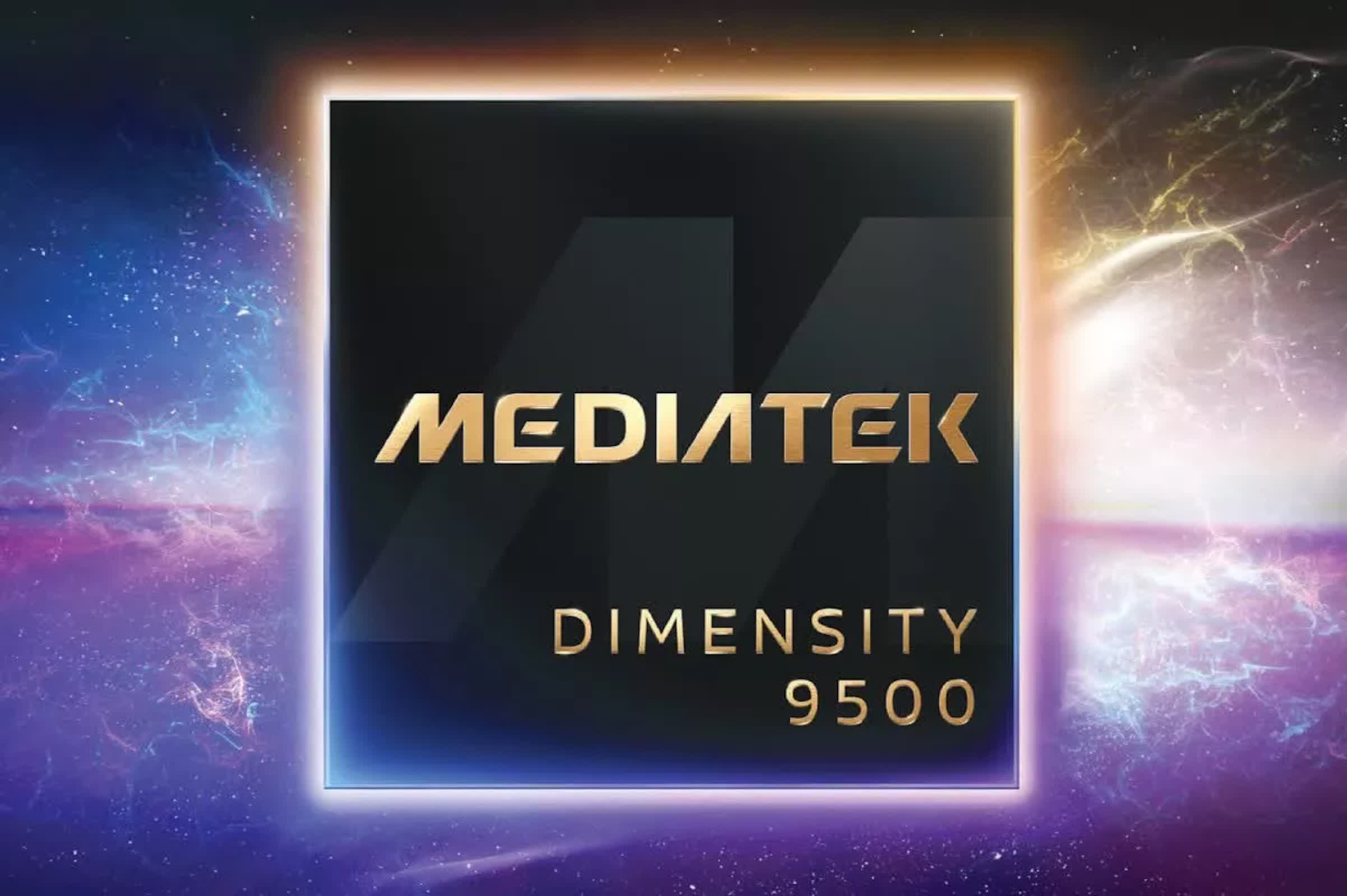
MediaTek's popular Dimensity smartphone chip line remains competitive in the near term. Both MediaTek and Qualcomm are adopting TSMC's N2P 2-nanometer process for their next flagship processors, a move that promises higher CPU clocks with improved efficiency.
But with fewer resources now directed toward smartphone silicon, analysts question how long MediaTek can maintain parity with Qualcomm's Snapdragon lineup, much less challenge Apple's in-house A-series processors, which continue to dominate high-end performance.
MediaTek is shifting from smartphone chips toward a billion-dollar bet on AI ASICs