In the race to keep up with Moore’s Law, computer scientists and electrical engineers at Stanford University and MIT have published a paper in the journal Nature detailing a three-dimensional computer chip that integrates RAM into the CPU using carbon nanotubes. The team has produced a small-scale carbon nanotube (CNT) computer, capable of running programs, a basic multi-tasking operating system, and performing MIPS instructions. Project lead Max Shulaker believes that the technology can overcome bottlenecks in communication between logic circuits and memory.
The problem facing engineers today is not so much one of how to increase processing power or storage capacity as it is one of how to pass large volumes of data back and forth. The fastest CPU and RAM is still only as fast as the bus. While advancements in processors and memory are still being made, communication between the two is a looming limitation. As the volume of data that needs to be processed increases (think 4K+ video), the more congested the lines of communication become. So processing speed will eventually become hampered by the physical limitations of parallel communication.
"[The CNT computer is] the most complex nanoelectronic system ever made with emerging nanotechnologies."
The Stanford/MIT research team believe the answer to this problem is building 3D chips that have “interleaving layers of logic and memory.” Not only have they demonstrated that this technology is possible, but they have also fundamentally changed the way that transistors will be fabricated.
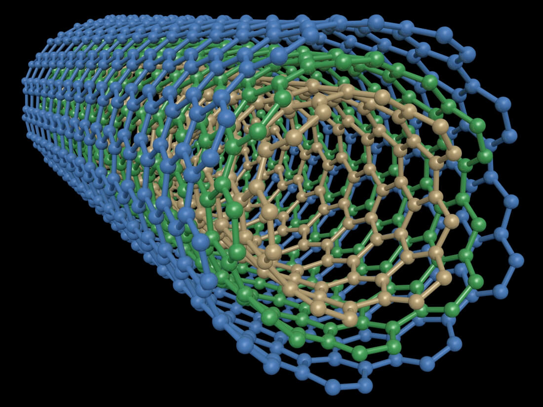
Instead of being made from silicon, the transistors are made from graphene, more specifically, the nanotubes created by the graphene. They are called “carbon nanotube field-effect transistors” (CNFET), and they provide the logic layer within the chip.
The other layer of the processor is the “resistive random-access memory” (RRAM). RRAM works by altering the resistance of a solid dielectric material. "RRAM can be denser, faster, and more energy-efficient compared to DRAM," says H.-S. Philip Wong, a co-author of the research.
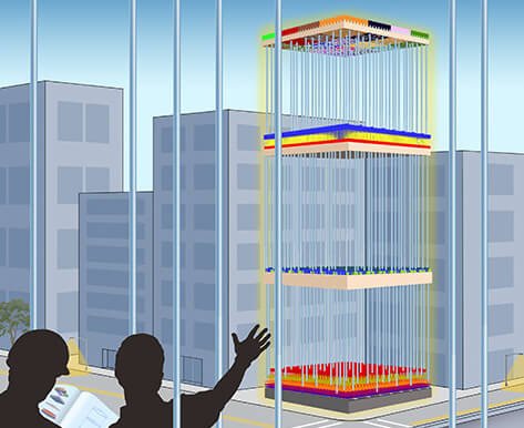
Rendering of the layers of the CNT chip with nanotube lines of communication between the layers.
In-between the logic and memory layers are “ultradense" wires that provide communication, which is “more than an order of magnitude” faster and more energy efficient than silicon. It's like the jump from serial to parallel processing, only here the parallel lines are being multiplied (above image). Although the carbon nanotube (CNT) computer is nowhere near as fast as current CPUs at this point in the research, this is a trivial matter according Shulaker.
“Although CNFET circuits promise improved speed, our computer runs at 1 kHz. This is not due to the limitations of the CNT technology or our design methodology, but instead is caused by capacitive loading introduced by the measurement setup, the 1-mm minimum lithographic feature size possible in our academic fabrication facility, and CNT density and contact resistance. The CNT computer operates on single-bit data values, this is not a fundamental limitation, because any multibit computation can be performed with a single-bit computer through serial computation. Additionally, having shown the ability to cascade logic, fabricating a larger multibit CNT computer is not a fundamental obstacle.”
Even with the lab’s limited fabrication capabilities, “the researchers integrated over 1 million RRAM cells and 2 million carbon nanotube field-effect transistors, making the most complex nanoelectronic system ever made with emerging nanotechnologies.”
The team has constructed something that is not possible to create using silicon. Building a 3D architecture with silicon is problematic due to the heat involved in fabricating the transistors. Silicon transistors are made at temperatures as high as 1,000 degrees C. Trying to build them in layers will damage the previous layers. Conversely, nanotube circuits and RRAM can be produced at temperatures of around 200 degrees C. “This means they can be built up in layers without harming the circuits beneath,” said Shulaker.
The research is being funded by the Stanford SystemX Alliance, which is comprised of numerous large corporations such as Google, Samsung, IBM, and more. The Defense Advanced Research Projects Agency, the National Science Foundation, Semiconductor Research Corporation, and STARnet SONIC are also helping fund the project. With so many interested parties contributing, we may start seeing CNT computers and other devices sooner than we think.
https://www.techspot.com/news/70036-mit-stanford-created-3-d-chip-integrating-processing.html
