Next-gen Nvidia Rubin prototypes begin testing with leap to chiplet design and HBM4 memory

Skye Jacobs

Posts: 1,913   +58
Staff
Forward-looking: Initial Nvidia Rubin prototypes have entered qualification at TSMC. Industry watchers and cloud operators are following closely, recognizing that the platform could set the trajectory for the next era of high-performance computing. Far more than a routine chip update, Rubin represents a sweeping architectural shift that may determine how future AI models and hyperscale data centers are built and scaled.

Nvidia has confirmed the completion of six Rubin chips, marking a major strategic shift in its technology roadmap. The announcement came during CEO Jensen Huang's recent visit to Taiwan, where he revealed that multiple designs have already been submitted to manufacturing partner TSMC for qualification and initial production runs.

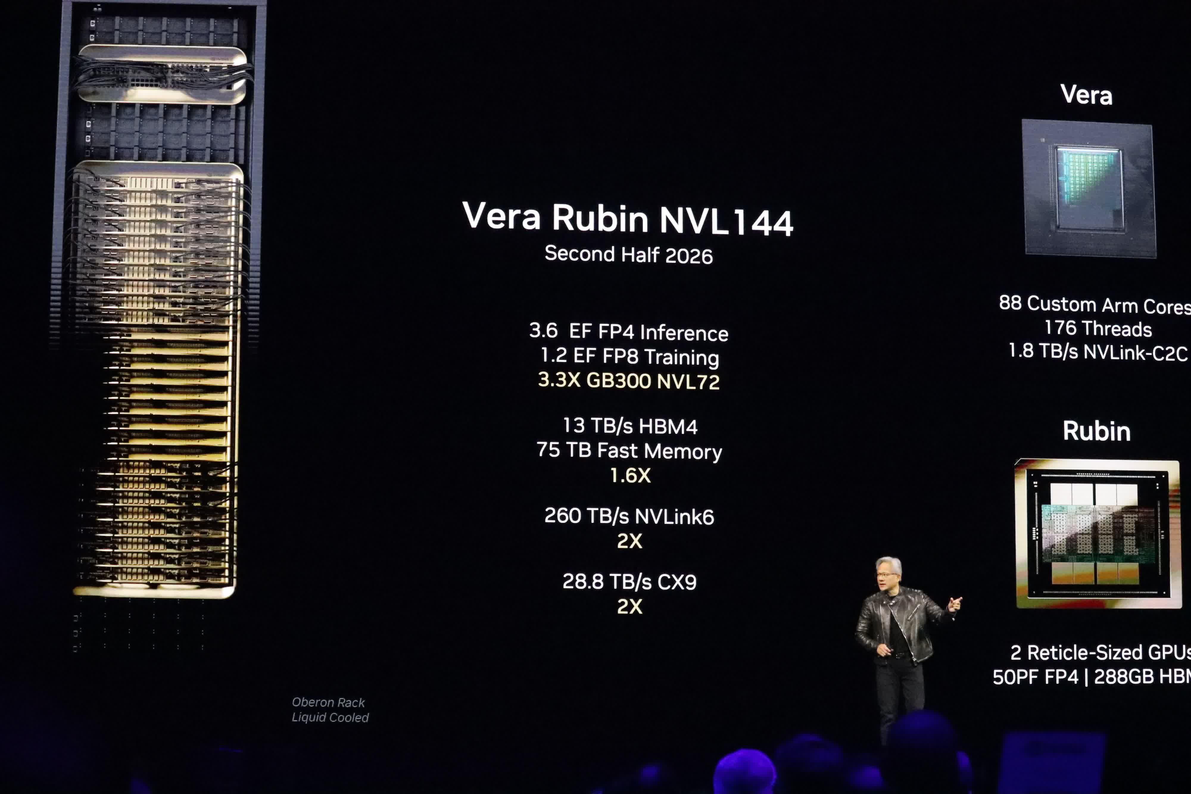
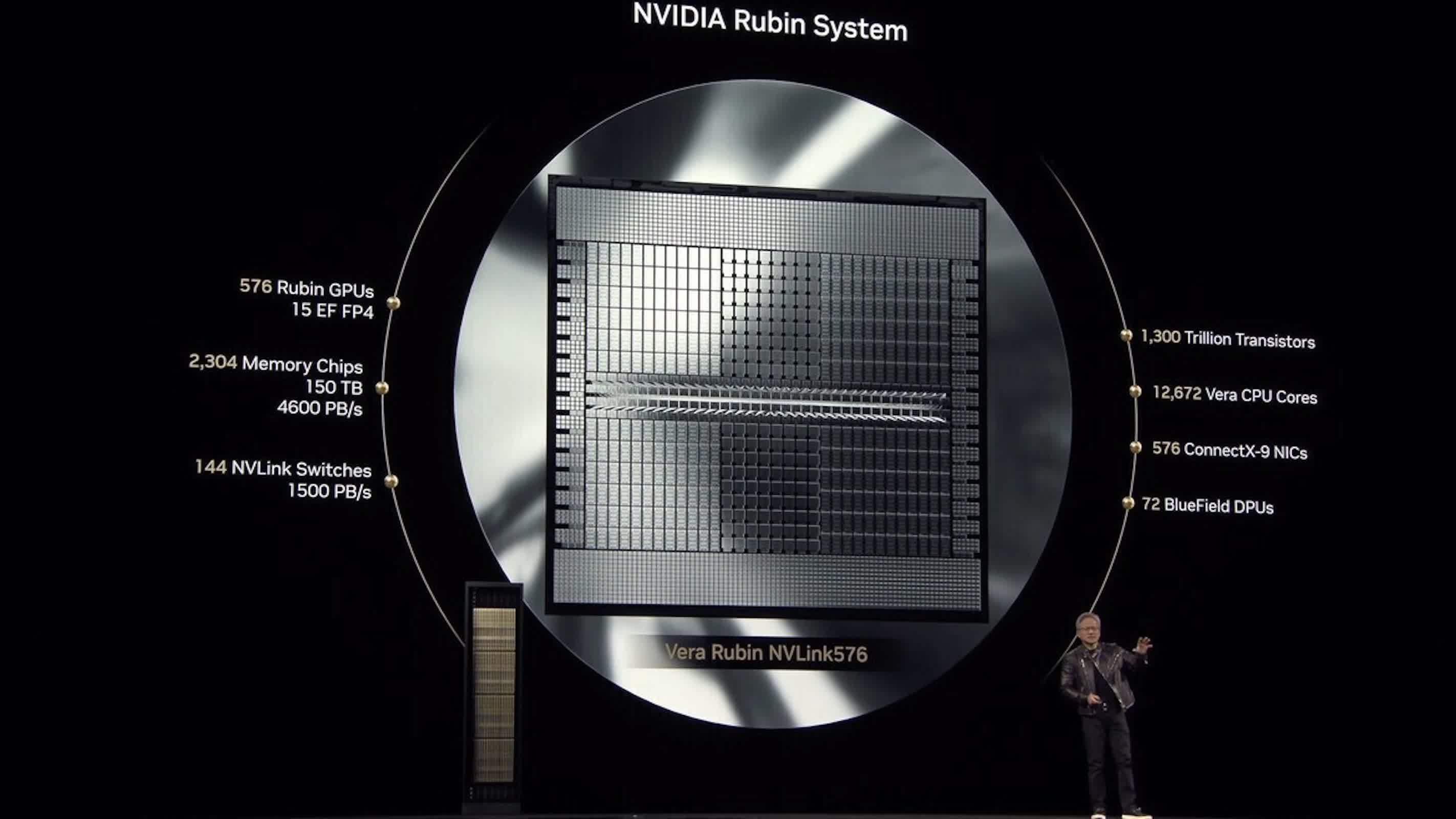
Unlike standard product refreshes that focus on incremental component upgrades, Rubin represents a platform-wide advance spanning processors, networking hardware, and interconnect technology.

Rather than being just another GPU update, Rubin is a comprehensive overhaul of Nvidia's compute infrastructure. The new platform introduces chiplet partitioning – a significant first for the company – and will leverage TSMC's advanced N3P fabrication process in combination with CoWoS-L packaging.

Huang explained that the lineup includes a dedicated CPU, several GPU variants, a scale-up NVLink switch for higher data throughput, a networking chip, a switch, and a silicon photonics processor designed to enhance rack-scale connectivity and off-chip optical links.

Huang emphasized his gratitude to TSMC staff, noting, "I came to thank all of their operations people for working so hard for me."

In addition to hardware innovation, Nvidia is coordinating major changes to supporting software, including updates to compilers and runtime systems that will fully exploit the new chip architecture. The Rubin platform will transition to next-generation HBM4 memory stacks, featuring customized base die designs to sustain higher bandwidth and increased computational requirements. The physical compute dies themselves will be larger than those found in the current product generation.

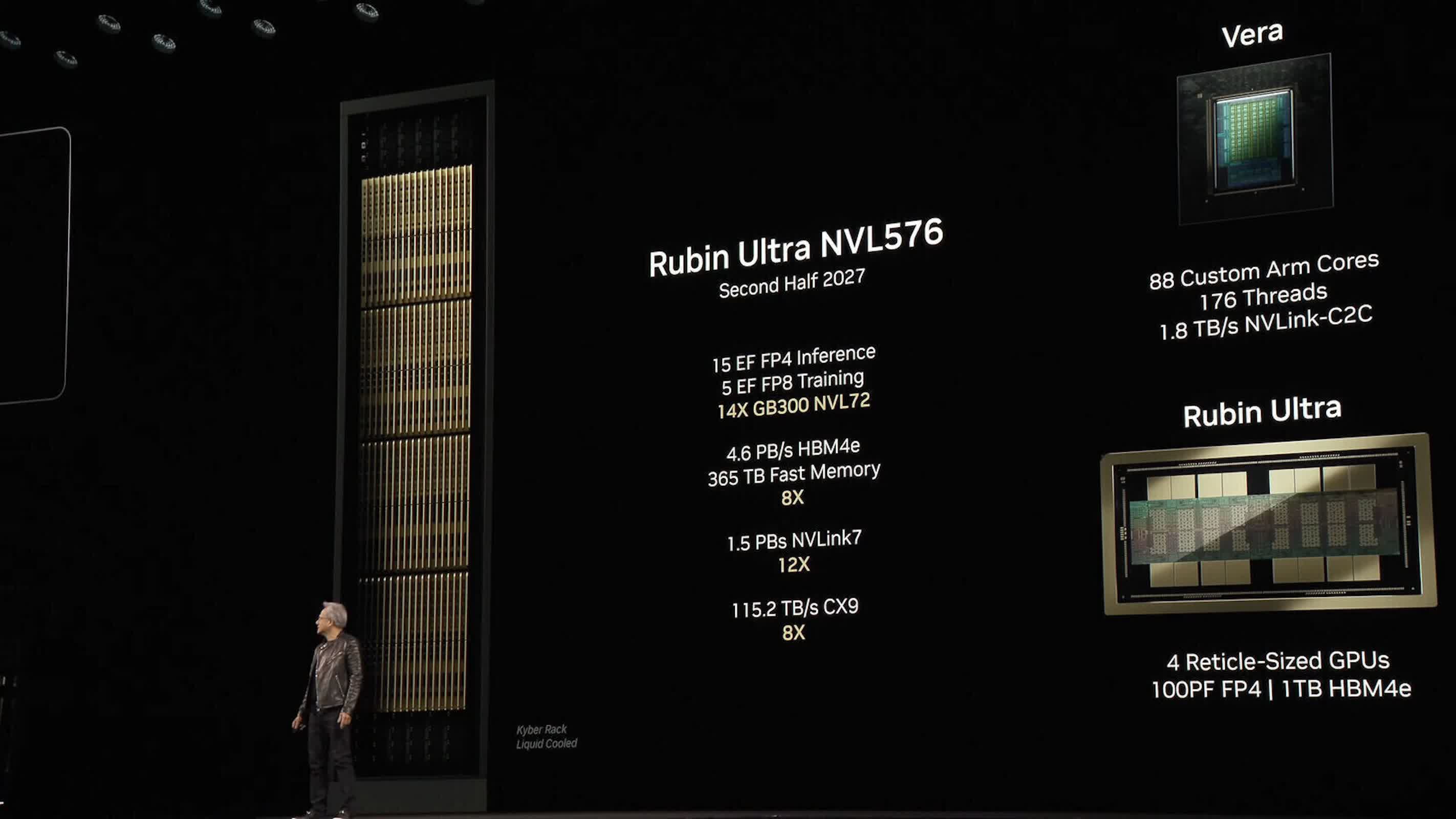
Nvidia has already entered early validation for the new chips, running tests on thermal performance, power consumption, and interconnect efficiency. The company expects market introduction for the Rubin family around 2026, with Rubin Ultra anticipated in 2027, both timelines subject to manufacturing yields and fab readiness.

The launch of Rubin comes as hyperscale data centers and AI workloads demand unprecedented computational capacity – what some in the industry now describe as "AI token factories."

Nvidia's new chips are positioned to enable breakthroughs in massive data environments, supporting millions of active units and next-generation AI applications.

Permalink to story:

 
This is what a company like Intel is missing. Nvidia is already on the top of the pile.

They can easily keep doing what they've been doing with minor performance updates for the next 10 years and no one (even AMD) will be able to catch up to them in that time because they've been sowing these seeds for the last 20 years with CUDA.

But they don't and they're going to do chiplet packaging now too?

Good lord AMD's instinct just lost the one minor advantage it had over Nvidia's enterprise line...
 
The author is confusing a package of monolithic components, for a chiplet design. The use of reticle sized monolithic GPU dies, is definitely not a chiplet design. The Rubin package, that includes a multicore ARM CPU, uses a monolithic die for the entire CPU. There's nothing "chiplet" going on with Rubin that I see, the design choices are similar to Blackwell, using a large sized package, to accommodate a maximum of 4 reticle limit sized GPU dies, a CPU die, HBM memory, and the necessary interconnections.
 
The author is confusing a package of monolithic components, for a chiplet design. The use of reticle sized monolithic GPU dies, is definitely not a chiplet design. The Rubin package, that includes a multicore ARM CPU, uses a monolithic die for the entire CPU. There's nothing "chiplet" going on with Rubin that I see, the design choices are similar to Blackwell, using a large sized package, to accommodate a maximum of 4 reticle limit sized GPU dies, a CPU die, HBM memory, and the necessary interconnections.


The author is not alone as even Jensen Huang says Rubin will be chiplet design using 6 complex "chiplets" onto the CoWoS package. Does it matter if the tiles are large or small? There are multiple tiles using interconnect technology. It may not be at Intel's level of tile complexity but sounds like you are talking semantics.
 
The author is not alone as even Jensen Huang says Rubin will be chiplet design using 6 complex "chiplets" onto the CoWoS package. Does it matter if the tiles are large or small? There are multiple tiles using interconnect technology. It may not be at Intel's level of tile complexity but sounds like you are talking semantics.

One of the key characteristics of a "chiplet", is that it's cut out from a full die, as opposed to being the full die, several identical chiplets are produced per die. Teh advantages, are that a defect does not ruin everything, several chiplets will be fine, another advantage, is that different nodes can be used where there's an advantage (or no advantage) rather than, one node must fit all. The embellishment of the chiplet terminology, is done intentionally, because Nvidia does not have the equivalent capability to produce chiplets, all they know, is how to make full dies at the reticle limit. What's telling, is that not having chiplets makes them look bad, that is why that are trying to claim they have a similar chiplet capability when they clearly do not.
 
Back