Nvidia's Pascal GP104 GPU may opt for GDDR5 over HBM

Scorpus

Posts: 2,159   +239
Staff member

A recent shipment of what appears to be Nvidia's upcoming Pascal GPU from Taiwan to Bangalore has revealed some possible information about the chip before its launch later this year.

The shipment information suggests that Nvidia's GP104 Pascal GPU will be 37.5 x 37.5 mm and will feature 2,152 pins. While there's no firm information to confirm such a move, the surprisingly small die size indicates Nvidia will not use high-bandwidth memory (HBM) along with this GPU.

The reason why it appears Nvidia will not use HBM with the GP104 is that a die of this size could not accommodate both a high-performance GPU and the HBM chips, which sit on the same substrate. Instead, current speculation suggests GP104 graphics cards will use GDDR5 or GDDR5X, resulting in less memory bandwidth than a HBM solution.

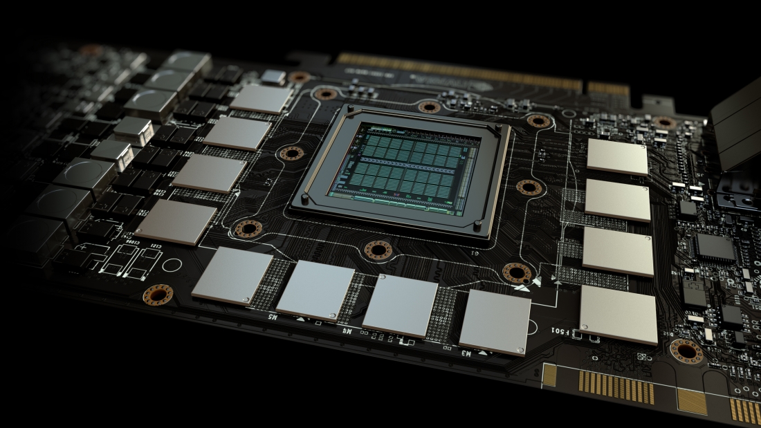
Meanwhile, the top-end GP100 GPU is expected to come in at 55 x 55mm, which is larger than the Maxwell-based GM200 (seen above). Factoring in a manufacturing process shrink to 16nm, GP100's extra die size will likely be used to accommodate HBM, making it Nvidia's first GPU to use the technology.

Pascal is still several months away, and the information in this latest report is far from concrete, so it should be taken with a grain of salt. However it shouldn't be too long before we get a look at what Nvidia has in store for 2016.

Permalink to story.

 
So basically only Nvidia's top end will be using HBM2.
I'm ok with that, I doubt the lower end cards would fully utilize all the bandwidth HBM2 has to offer anyway so this just means Nvidia can keep production costs in check.
 
So basically only Nvidia's top end will be using HBM2.
I'm ok with that, I doubt the lower end cards would fully utilize all the bandwidth HBM2 has to offer anyway so this just means Nvidia can keep production costs in check.
More importantly that means there will hopefully be more HBM2 to go around for those top end cards, hopefully keeping prices from inflating due to supply issues (as much).
 
I think it's a good idea to do a staggered roll-out of HBM like this. Gives devs time to take advantage of the HBM tech.
 
They said pascal will be 10 times more powerful than maxwell.let's wait and see, but I think amd will do better in midrange.
 
This is good news...for AMD; and I'll most likely be in the market for a serious GPU upgrade sometime in June/July. Perhaps it's AMD that will get my business this time around.
 
Games are first & foremost coded for wheezy consoles and their hardware is decrepit anyway so HBM shouldn't make much of a difference anytime soon.
 
This is good news...for AMD; and I'll most likely be in the market for a serious GPU upgrade sometime in June/July. Perhaps it's AMD that will get my business this time around.
AMD might not release high end cards this year. We'll just have to wait and see.
 
There is something WRONG with this piece.

"the surprisingly small die size indicates Nvidia will not use high-bandwidth memory (HBM) along with this GPU."

Actually 37mm is in fact too LARGE to be used with an interposer. As AMD's Fiji at 28nm was only 21mm each side and quite successfully released as the first to use HBM on a 28nm Fiji GPU. The interposer for Pascal would be huge and very expensive.

Does this mean that Pascal is NOT 16nm? Probably.

There is another reason and that would be HBM2 is likely not ramping up to production as well as expected as AMD is also releasing an "entry level" 14nm Polaris GPU also with DDR5. Thus saving the HBM2 for higher performing "enthusiast" and workstation cards. The GPU with HBM2 is an assembly. Perfectly good GPU's can be lost with a failed interposer assembly. I suspect they are the last component to be assembled.

The real story is Pascal is HUGE. So what does that tell us about the process?
 
This is good news...for AMD; and I'll most likely be in the market for a serious GPU upgrade sometime in June/July. Perhaps it's AMD that will get my business this time around.
AMD might not release high end cards this year. We'll just have to wait and see.


AMD is releasing Polaris with DDR5 by summer and Polaris with HBM2 will pop up for Christmas just as Fiji did. In fact Polaris is already shipping. Polaris is also 14nm process.
 
This is good news...for AMD; and I'll most likely be in the market for a serious GPU upgrade sometime in June/July. Perhaps it's AMD that will get my business this time around.


You should see the 14nm Polaris well before June. And Polaris with HBM2 shortly after.
 
There's also speculation floating around about Pascal having yield problems too since it was absent from the Drive PX2 showing. So whether or not this is specific to GP104 or Pascal as a whole remains to be seen. I doubt Nvidia would stick with GDDR5X though even for the top end cards, especially with AMD likely doing it again.
 
There's also speculation floating around about Pascal having yield problems too since it was absent from the Drive PX2 showing. So whether or not this is specific to GP104 or Pascal as a whole remains to be seen. I doubt Nvidia would stick with GDDR5X though even for the top end cards, especially with AMD likely doing it again.

Pascal at 37mm is far too large and THAT is the real story. AMD Fiji was only 21mm with the 28nm process as well. 14nm Polaris is much smaller.
 
HBM2 is not cheap the makers think they have Nvidia in a bind to use it. But it is only needed if you want a smaller card the performance to D5 is not that much. The whole purpose is to make Lots of Money and H ram takes that away. Sure they will use H ram when the Chip maker not so Greedy.
 
Considering 7GHZ GDDR5 held its own against Fiji, this doesn't worry me yet.
Chances are that Nvidia's (and possibly AMD's) upper mainstream cards will end up using GDDR5X, so the 9500-10000MHz effective speed should offset the increasing bandwidth requirements. As you say 7Gbps GDDR5 works out fine for Titan X/980 Ti, so even if GP 104's GPU performance is higher (I doubt by much), GDDR5X will still be a viable solution.
AMD might not release high end cards this year. We'll just have to wait and see.
I think AMD are aiming at a top-to-bottom architecture revamp (their first for a while) over H2 2016. Their first or second tier GPU is already doing the marketing rounds.
There is something WRONG with this piece.

"the surprisingly small die size indicates Nvidia will not use high-bandwidth memory (HBM) along with this GPU."

Actually 37mm is in fact too LARGE to be used with an interposer. As AMD's Fiji at 28nm was only 21mm each side and quite successfully released as the first to use HBM on a 28nm Fiji GPU. The interposer for Pascal would be huge and very expensive.
Wow, you have so much wrong it's difficult to know where to start.
Fiji is 596mm² - that is 24.4mm per side NOT 21mm (which equals 441mm²). The Interposer used is 1011mm² (31.8mm per side).
The interposer is made by UMC and represents a first-gen attempt at 2.5D integration. Companies like ASE (PDF)and TSMC are well on their way to producing not only second generation interposers of sizes only constrained by wafer size, but full assembly including better integrated X-ray metrology for QA/QC purposes.
This QA/QC stage is the principle cost factor (tooling, time, yield of viable TSV's and soldered microbump contacts) NOT the interposer itself as the slide below illustrates- which is fairly cheap and made on a fairly old 65nm process so can repurpose tooling/fabs currently churning out chipsets and microcontrollers.
BiNQWrw.jpg


Does this mean that Pascal is NOT 16nm? Probably.
Sorry to burst your bubble, but Pascal has been sighted and confirmed by numerous sources as being fabbed and shipped on TSMC's 16nmFF+, and is currently undergoing test, verification, and validation.
The real story is Pascal is HUGE. So what does that tell us about the process?
Absolutely nothing. Here's an example:
596mm Fiji (28nm)
334mm Cypress (40nm)
420mm R600 (90nm)
289mm R423 (130nm)
or if you're talking Nvidia only:
601mm GM200 (28nm)
529mm GF100 (40nm)
576mm GT200 (65nm)
484mm G80 (90nm)

The only thing you can extrapolate for the die sizes is that 1. TSMC's (and nearly everyone else's) litho tooling reticule limit is the limiting factor in die size (around 625mm² per die), and 2. Die area is governed by the features the vendor shoehorns into the chip floorplan.
 
Last edited:
So basically only Nvidia's top end will be using HBM2.
I'm ok with that, I doubt the lower end cards would fully utilize all the bandwidth HBM2 has to offer anyway so this just means Nvidia can keep production costs in check.

Yup, especially if Pascal uses 4th generation memory compression tech. I predict at the start of the new node (14/16nm), both AMD/NV will release cards 20-40% faster than 980Ti/Fury X but not much more. I am expecting die sizes of 290-375mm2 tops. This is in line what both companies did with Kepler 680/GCN 7970 when they shifted to brand new 28nm node. Both AMD and NV will try to maximize profits/margins which means selling mid-range die chips at flagship prices. Then, we should see the larger die true flagships drop in late 2016 or 1H 2017.

Recalling NV's Kepler and Maxwell generations, this is what they did:
- Mid-range 680 @ $500
- Cut-down large die Titan @ $1000
- Cut-down large die 780 @ $650
- Finally large die real flagship 780Ti @ $700

Maxwell: mid-range 980 @ $550, then cut-down flagship 980Ti @ $700.

The old days of flagship card beating last gen's card by 1.7-2X are over. Now, both firms will release several 'flagships' at $550-650 over the course of a generation -- let the milking commence!
 
I just noticed that the author seems to be confusing GPU size with package size. The latter is the completed assembly size and includes the GPU bracing and mounting assembly.
For example, GK 104 is a 294mm² chip while GM 204 is 398mm², but the package for both is 40mm x 40mm (1600mm²). GM 200's package size is the same as GK 110's at 45mm x 45mm while the chip itself is 24.5mm x 24.5mm
4MkPGQi.jpg

[Source: Quadro M6000 Specification -PDF)

I would be very wary of trying to extrapolate too much from package size. More often than not the reasoning for package size is predicated upon other factors such as OEM's and third parties ( especially for PCB layouts and cooling compatibility)
 
Chances are that Nvidia's (and possibly AMD's) upper mainstream cards will end up using GDDR5X, so the 9500-10000MHz effective speed should offset the increasing bandwidth requirements. As you say 7Gbps GDDR5 works out fine for Titan X/980 Ti, so even if GP 104's GPU performance is higher (I doubt by much), GDDR5X will still be a viable solution.

I think AMD are aiming at a top-to-bottom architecture revamp (their first for a while) over H2 2016. Their first or second tier GPU is already doing the marketing rounds.

Wow, you have so much wrong it's difficult to know where to start.
Fiji is 596mm² - that is 24.4mm per side NOT 21mm (which equals 441mm²). The Interposer used is 1011mm² (31.8mm per side).
The interposer is made by UMC and represents a first-gen attempt at 2.5D integration. Companies like ASE (PDF)and TSMC are well on their way to producing not only second generation interposers of sizes only constrained by wafer size, but full assembly including better integrated X-ray metrology for QA/QC purposes.
This QA/QC stage is the principle cost factor (tooling, time, yield of viable TSV's and soldered microbump contacts) NOT the interposer itself as the slide below illustrates- which is fairly cheap and made on a fairly old 65nm process so can repurpose tooling/fabs currently churning out chipsets and microcontrollers.
BiNQWrw.jpg


Sorry to burst your bubble, but Pascal has been sighted and confirmed by numerous sources as being fabbed and shipped on TSMC's 16nmFF+, and is currently undergoing test, verification, and validation.

Absolutely nothing. Here's an example:
596mm Fiji (28nm)
334mm Cypress (40nm)
420mm R600 (90nm)
289mm R423 (130nm)
or if you're talking Nvidia only:
601mm GM200 (28nm)
529mm GF100 (40nm)
576mm GT200 (65nm)
484mm G80 (90nm)

The only thing you can extrapolate for the die sizes is that 1. TSMC's (and nearly everyone else's) litho tooling reticule limit is the limiting factor in die size (around 625mm² per die), and 2. Die area is governed by the features the vendor shoehorns into the chip floorplan.


37.5mm is Massive. unless THE AUTHORS HAVE IT WRONG.
You seem confused about what I ACTUALLY wrote regarding AMD's success with an interposer. I made no mention of cost at all.
I also indicated that Fiji was 211mm per side which cam from here:

http://wccftech.com/amd-fiji-die-reconstructed-hbms-huge-gpu-uncovered/

and maybe wcctech got it wrong but you are quibbling over 3 mm or so hardly worth getting your panties in a twist over. And again I was ssaying NOTHING about AMD GPU on the interposer except it was a success. Why are you ranting so?

I also said that there was something WRONG with the piece and ANYONE with a 6th grade education would have picked up on the syntax problem.

"...the surprisingly small die size indicates Nvidia will not use high-bandwidth memory (HBM) along with this GPU."

The die size is FAR from small, it is massive. it is 37.5mm x 37.5 each side which is 1406.25 mm square. What is your point about die size. Unless the authors are WRONG.

As I said, something is wrong with this piece. the NVidia GPU is TOO big, not too small for the interposer.

So chill out, work on your reading comprehension, and lighten up. OK??
 
37.5mm is Massive. unless THE AUTHORS HAVE IT WRONG.
37.5mm * 37.5mm is the package size NOT the size of the GPU. Please read the post directly above yours for the clarification
You seem confused about what I ACTUALLY wrote regarding AMD's success with an interposer. I made no mention of cost at all.
I'm not confused at all. You said:
Actually 37mm is in fact too LARGE to be used with an interposer.
Rather than recapitulate, I'll simply say "No it isn't". The package can be larger than the interposer - as is the case with AMD's Fury.
I also indicated that Fiji was 211mm per side which cam from here:

http://wccftech.com/amd-fiji-die-reconstructed-hbms-huge-gpu-uncovered/
Well, there's your problem right there. Why use guessed data from an unreleased product, when the actual reviews carried either the AMD press deck or the full specification...or both is readily to hand?
AMD-Radeon-Fiji-Presentation-2.jpg
and maybe wcctech got it wrong but you are quibbling over 3 mm or so
That 3mm is the difference between a GPU measuring 441mm² and 596mm². That is basically the difference between AMD's Hawaii and Fiji. Hardly trivial.
And again I was ssaying NOTHING about AMD GPU on the interposer except it was a success. Why are you ranting so?
It is hardly ranting. You made the assertion:
The interposer for Pascal would be huge and very expensive
I merely pointed out that interposers aren't expensive.
What is expensive - although getting cheaper as QA tooling comes online - is the package assembly. If you consider me or anyone else correcting your assumption ranting, then either make sure you have the correct information to hand or develop a thicker skin.
I also said that there was something WRONG with the piece and ANYONE with a 6th grade education would have picked up on the syntax problem.
The problem with the article is that it doesn't differentiate between GPU die size and GPU package size (as I outlined in the post immediately above yours) - but even a cursory glance at the source link in the article (PC Perspective) would confirm that the shipping manifest was talking about the entire GPU package - which includes not just the GPU but the IHS, mounting and bracing hardware.
So chill out, work on your reading comprehension, and lighten up. OK??
I think it might be you that needs the chill pill. So the author made a mistake in terminology? Big deal. Spending a few seconds reviewing the source material would very quickly show that the figures related to the assembled package size and not the bare GPU. Coming across all indignant because you couldn't be bothered clicking a source link to cross check before posting makes it seem like you are the one going off half-cocked.
As for your assertion that a difference in 3mm per side of a large GPU is "quibbling"...you obviously haven't thought that through particularly well. That difference is 155mm² and represents a larger die size greater than 50% of all GPU designs, a difference that actually exceed the entire die size of GM 107 (GTX 750Ti), and is comfortably larger than the Cape Verde GPU that powers the HD 7770/ R7 250X

Anyhow, have a nice day :)
 
Who are we kidding? Samsung was going to supply nVidia with HBM memory. nVidia blew it with their lawsuit against them. Aside from that, nVidia was infringing on Samsung's patents. Samsung not making HBM for nVidia will force nVidia to think of alternatives.
 
Who are we kidding? Samsung was going to supply nVidia with HBM memory. nVidia blew it with their lawsuit against them. Aside from that, nVidia was infringing on Samsung's patents. Samsung not making HBM for nVidia will force nVidia to think of alternatives.
That won't make any difference. Business is business. Samsung and Apple have been engaged in one of the longest and most bitter patent battle in history - far exceeding what Samsung/Nvidia amounted to - yet Samsung and Apple continue to do business. Another example would be that AMD and LG are currently also involved in a patent lawsuit - it doesn't stop LG incorporating FreeSync and helping AMD raise its brand awareness.
Multi billion dollar businesses aren't run like forum fanboy wars or toddlers pitching tantrums. The bottom line is doing business. There are literally hundreds of patent and copyright battles being fought in courts all over the world involving companies that still do business and continue to sign new contracts.

Another thing to consider is that Samsung don't deal with Nvidia directly. Samsung's contract will be with the OEMs tasked with manufacturing the cards - Hon Hai (Foxconn) for the reference card, and AIB's and ODM's (EVGA, Asus, MSI, Gigabyte, PC Partner, Palit etc.) for custom cards.

The other more obvious issue is that the contract for Samsung to provide HBM would have been signed well before the current legal spat with Nvidia. Breach of contract would be the least of Samsung's problems since attempting to scupper Nvidia's flagship would also greatly affect the Nvidia/IBM/Mellanox contract with the U.S. government and be an instant candidate for anti-trust sanctions.
 
Last edited:
Back