Scientists develop semiconductor-free microelectronics

Shawn Knight

Posts: 15,285   +192
Staff member

A team of engineers within the Applied Electromagnetics Group at the University of California San Diego have developed what they are calling the first semiconductor-free, optically-controlled microelectronic device.

Translation – they’ve essentially created modern-day vacuum tube technology in nanoscale that could possibly replace the speed, wavelength and power handling of microelectronics beyond what is possible with today’s semiconductors.

The problem with semiconductors, the team highlights, is that they can impose limits on a device’s conductivity (electron flow). They also have a band gap meaning they require a boost of external energy to get electrons flowing through them. Because electrons are constantly colliding with atoms as they flow through the semiconductor, electron velocity is limited.

The engineering team wanted to remove this roadblock by replacing semiconductors with free electrons in space at the microscale. Doing so, however, requires either applying high voltages (a minimum of 100 volts), high-power lasers or extremely high temperatures (over 1,000° F) – none of which are practical in micro or nanoscale electronic devices.

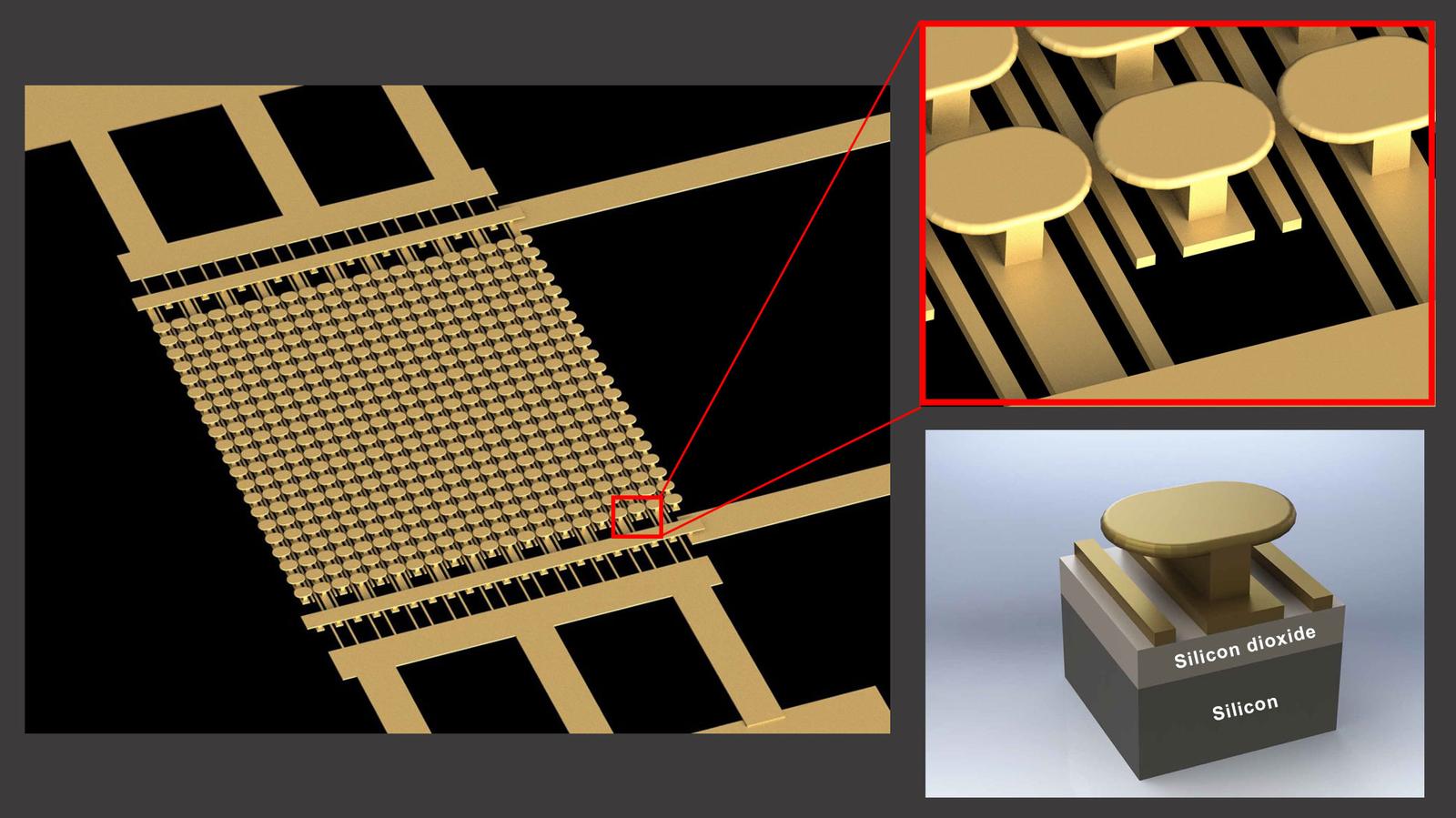
To circumvent the challenge, the team fabricated a metasurface on top of a silicon wafer with a layer of silicon dioxide between the two. The metasurface is unique in that it consists of an array of gold mushroom-like nanostructures on an array of parallel gold strips.

By applying a low DC voltage (less than 10 volts) and a low power infrared laser to the metasurface, it creates high-intensity electric fields that can free electrons in space.

Ebrahim Forati, a former postdoctoral researcher and first author of the study, said the proof-of-concept metasurface has exhibited a 1,000 percent change in conductivity in testing which means more available electrons for manipulation.

Team lead and electrical engineering professor Dan Sievenpiper said the method won’t replace all semiconductor devices but it might be the best approach for specialty applications such as those that require high amounts of power or those that operate at very high frequencies. The next step, he said, is to understand how far the devices can be scaled and the limits of their performance.

Permalink to story.

 
You'll probably never see this in any consumer devices. But it will probably make its way into military hardware one day - the US Army and Navy LOVES both high voltages and high frequency AC power. Neither plays nice with modern semi-conductors.
 
Tubes/valves are still very much alive in audio electronics as well as electric guitar amplifiers, we'll see what the future brings
 
I think it's a kind of confused high voltage area of electric preprogramed logic thru microswitches on silicon substrate, not micro vacuum tubes and such.More like tunnel diode logic.Just my two cents.
 
As the article mentions, that might be useful in power electronics. As for TTL (5Vdc) semiconductor electronics, a replacement for the silicon transistor is sought after, e.g. Bismuth or Graphene Transistor, etc.

Intel is currently pursuing what's called compound III-V semiconductors, where "indium arsenide" (for transistor n-channels) and "indium gallium antimonide" (for transistor p-channels) are to be grown as the top active layer over a silicon substrate instead of silicon over silicon, since silicon's electrical capabilities have been tapped for the most part. That III-V semiconductor single crystal layer has superior electrical properties and power efficiency over silicon at smaller transistor sizes.
 
You seems to have opinion without much knowledge. I can see it being used for fiber, car, power circuit etc.
The defense industry still uses vacuum tubes to handle switching and amplification - not because they are better, but because silicon simply can't handle the job. There are some semiconductors that can - like Gallium Nitride (GaN) - but they are still very new, expensive, and not "battle tested".

You might see it in the power grid, but that is still not a consumer product. Even then, the solutions we have there can handle the 50/60Hz and 110/120V just fine, and this solution doesn't seem to offer any marked efficiency improvements, just increased operational ranges - so I doubt a switch to this tech, unless it turns out to be much cheaper or much more reliable.

Cars for the most part don't deal with anything above 12V and a few Amps - not high power - which silicon can be made to handle. EVs and Hybrids do deal with higher voltages, but still, we have solid state and electromechanical tech that can handle their requirements.

Audiophile usage was one I hadn't considered, but it would need to show some kind of improvement over current tube-amps to catch on. The only reason we 'old' tech for high end audio is because it is still a smooth continuous signal, while semi-conductors are either noisy or use discrete signals - and tubes are very good at what they do. The downside for these lower power tubes is the expense involved because of low-volume production, so this new metamaterial semi-conductor isn't likely to catch on unless it is much cheaper than old-style vacuum tubes (doubtful, seeing as it is more complicated in design and principle: lasers, complicated nano-scale structures).

Fiber optics has zero usage for this: that is photons, not electrons. Pure signal, no power transmission.

And power circuits was what I first suggested, but the only ones operating at high frequencies and high powers, matching the usage description in the original paper itself, are military in nature. Military hardware was designed that way because they were first designed with vacuum tubes, but also for various system compatibilities: like S-band and X-band antennas, and other 'radio' tech. Now, to maintain compatibility, they still use those high powers and frequencies, even as they transition to solid state tech.
 
It sounds like there is a waveguide like pattern that has been impressed on the device, and this pattern is key to the device operating with a low power IR laser stimulating electron emission via the photoelectric effect.

My guess is that it is because of the dimensions of the waveguide that allow this device to operate as it does. In other words, the pattern on the waveguide is probably some multiple or fraction of the wavelength of the IR laser, and that is what really allows this device to work at 10V which, as I see it, is not a particularly high voltage. However, if the device has characteristics such as those that allow Power MOSFETS to be easily combined in series and parallel, then the applications may be wider than the scientists expect at this moment.

I would not be surprised to see further improvements in this technology by tuning both the waveguide and the material on which the waveguide is impressed. I.e., find a material with a lower ionization energy, or that is more easily excited with different wavelengths of laser light, or a combination of both by optimizing the waveguide pattern.

To me, it is an interesting development and one that would not exist in a society that views science as taboo. Without Einstein and the insight he revealed on the photoelectric effect, this device might not exist. https://en.wikipedia.org/wiki/Photoelectric_effect
 
Yeah, if this pans out to a viable product, it is going to huge for radar receivers/exciters, and anything else along those same lines.
 
Back