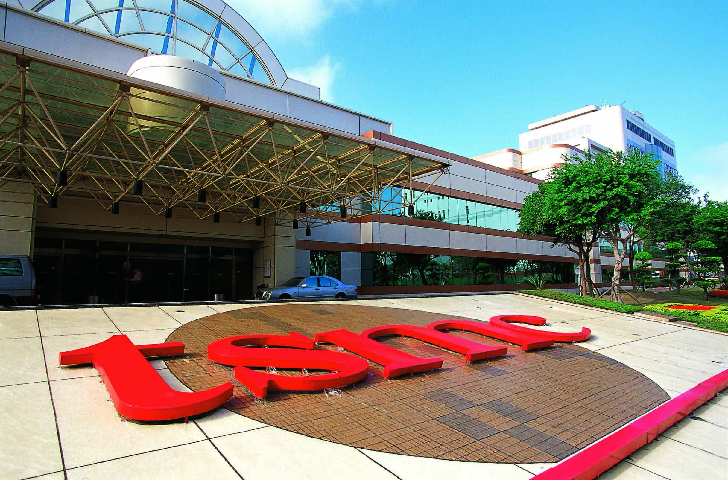
The big picture: Just days after Intel said it was optimistic about retaking process technology leadership by 2025, TSMC comes with an announcement that casts some doubt on that possibility. Competition in the semiconductor industry is heating up, and is even leading to odd partnerships where Intel is going to make chips for Qualcomm, while TSMC is racing to beat Samsung on the way to making 2nm chips.
This week, Intel offered more insights into its strategy to catch up with the rest of the semiconductor industry in terms of process technology, as well as the role played by the new Intel Foundry Services branch in achieving that goal. Unfortunately for Intel, who is hoping to catch up and then surpass the likes of TSMC, GlobalFoundries, Samsung, and others by 2025, this uphill battle looks increasingly difficult as time goes on.
Today, Nikkei reports that TSMC is planning to build a 2nm chip fab in Hsinchu, one of Taiwan's big chip manufacturing centers.
The company on Wednesday received the green light from the country's Environmental Review Committee to begin construction in early 2022. The second phase where the foundry equipment is installed could start as early as 2023.
The new facility will occupy 50 acres of land in the Hsinchu Science Park and is expected to start manufacturing 2nm chips in 2024. TSMC will gradually ramp up production as demand for the new process node grows, but the typical target for a GigaFab is 100,000 wafer starts per month.
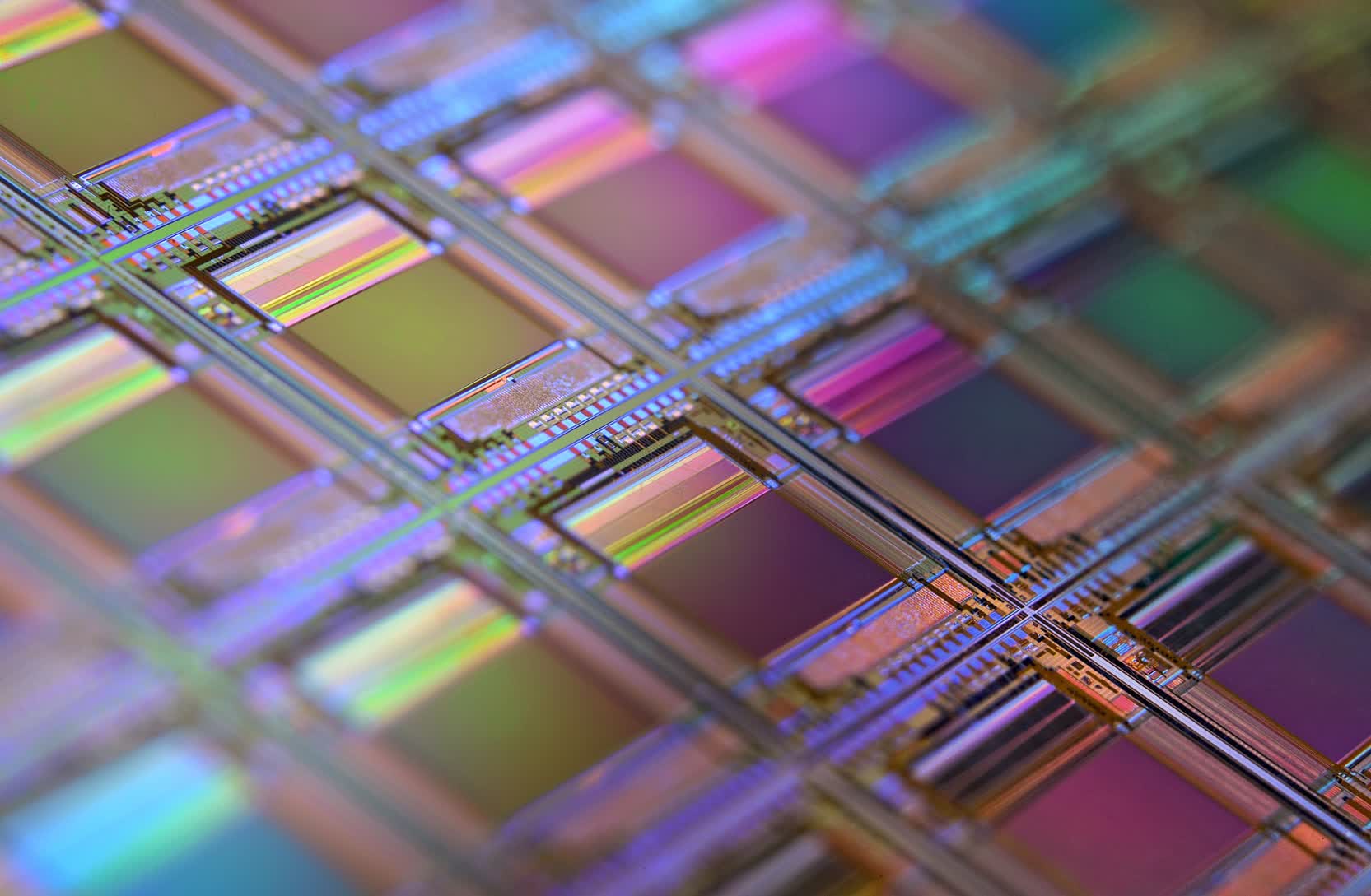
TSMC also has plans for a second 2nm GigaFab that could be established in Kaohsiung, at the Ciaotou Science and Industrial Park. The secret sauce of TSMC's N2 process technology is the use of gate-all-around (GAA) transistors, but the company is not yet prepared to reveal more details.
A more pressing problem is the water need of the new Baoshan facility, which is expected to use no less than 98,000 tons of water on a daily basis. To that end, TSMC set a goal to use 10 percent recycled water by 2025 and 100 percent reused water by 2030.
In the meantime, the construction of TSMC's N5 facility in Arizona is underway, as is the expansion of its 28nm fab in Nanjing, China. Additionally, the company is evaluating building more fabs in Germany and Japan.
https://www.techspot.com/news/90589-tsmc-gets-green-light-2nm-fab-plans-have.html
