TSMC reportedly on schedule for 3nm process fabrication line installation

Shawn Knight

Posts: 15,289   +192
Staff member
In context: Taiwan Semiconductor Manufacturing Company (TSMC) is on track to start volume producing chips based on its 3nm manufacturing process by the second half of 2022. If true, we could be on the cusp of a major advancement in mobile processing technology.

According to a recent report from DigiTimes, the semiconductor foundry “has been engaged in the installation of 3nm process fabrication lines and related facilities” and is still on schedule to complete the project as originally planned. TSMC will reportedly be ready for risk production next year ahead of the aforementioned volume production the second half of 2022.

Should these dates hold, it potentially means that one of TSMC’s biggest clients – Apple – could have its first 3nm-based SoC ready in time for inclusion in 2022 model iPhones.

In the interim, TSMC is said to be volume producing 5nm chips and is working on enhanced process variants. Apple’s next-gen iPhone, tentatively dubbed the iPhone 12, is expected to ship with a 5nm-based SoC that could be called the Apple A14 Bionic. Early benchmarks of the alleged A14 look promising and with 3nm on the horizon, we could soon be entering a new era in terms of power and efficiency previously unseen.

3nm is approaching the barrier of what might be possible in terms of die shrinks, at least for the foreseeable future. That said, it was reported last year that TSMC was looking into 2nm production. Intel, meanwhile, has a roadmap that involves 1.4nm production although not until 2029.

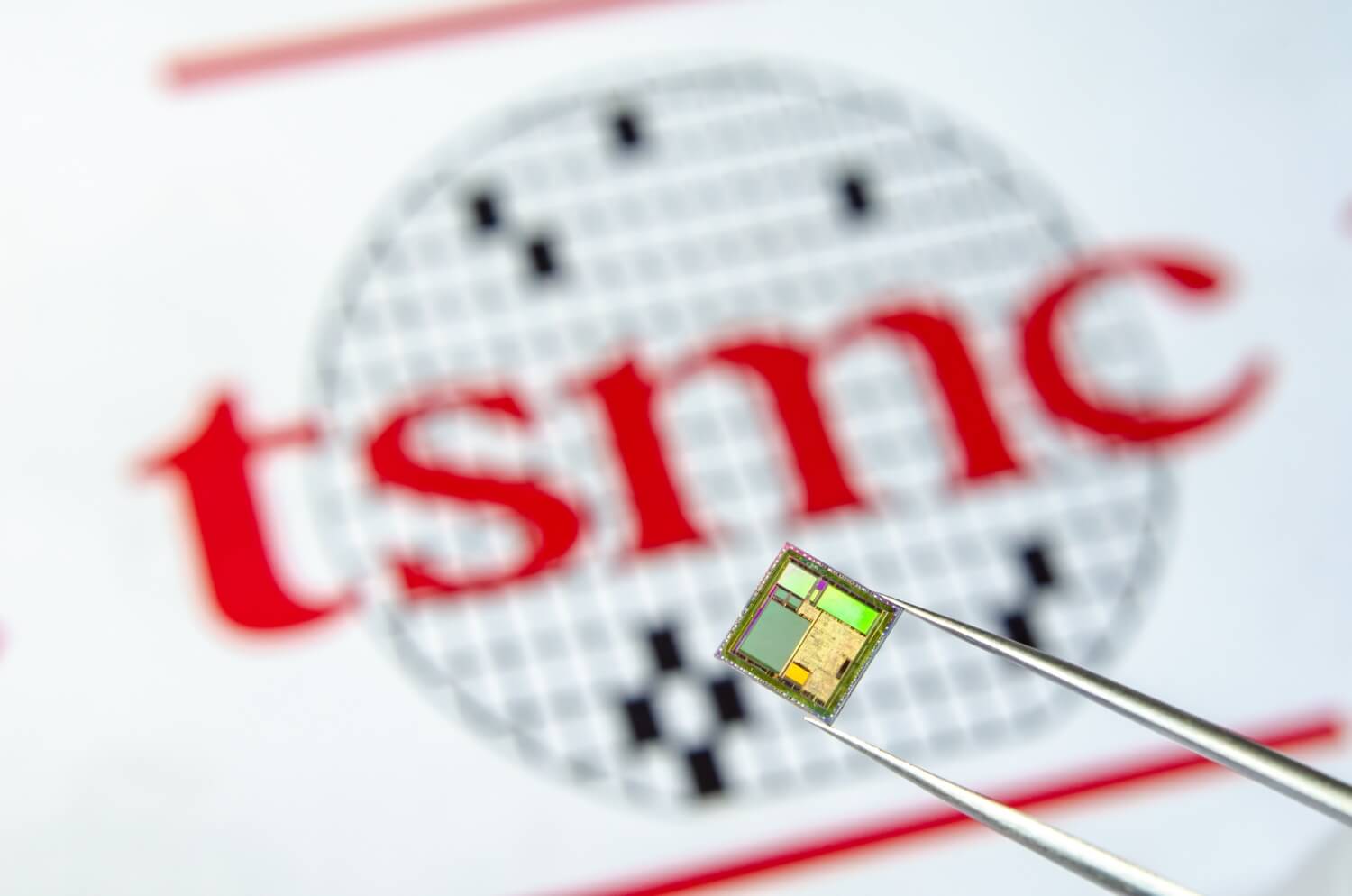
Masthead credit: Ascannio

Permalink to story.

 
I'd say: less than 1nm in less than 20 years.
Unlikely. The rate of electron tunneling increases exponentially as you linearly shrink the die, so exponential die shrinks just compound the exponential increase electron tunneling. While you can probably can shrink the die below 1nm, I doubt it will be economical to do so. We're going to hit a point in the next few years where increases in computing power solely come from improving architectures, instead of also being from die shrinks.
 
Unlikely. The rate of electron tunneling increases exponentially as you linearly shrink the die, so exponential die shrinks just compound the exponential increase electron tunneling. While you can probably can shrink the die below 1nm, I doubt it will be economical to do so. We're going to hit a point in the next few years where increases in computing power solely come from improving architectures, instead of also being from die shrinks.


It's not economically... in 2020 terms.

But in 2040 terms...
 
Unlikely. The rate of electron tunneling increases exponentially as you linearly shrink the die, so exponential die shrinks just compound the exponential increase electron tunneling. While you can probably can shrink the die below 1nm, I doubt it will be economical to do so. We're going to hit a point in the next few years where increases in computing power solely come from improving architectures, instead of also being from die shrinks.

We will move beyond standard solid state IMO in the longer term, but in the shorter term it will be software that has to do the heavy lifting for performance gains. Quantum tunnelling was actually supposed to be a deal breaker smaller than 10nm if you look at research articles from 20 years ago. Obviously they have a done a great job to mitigate the effect with things like high k-dielectrics, but it can only get you so far
 
We will move beyond standard solid state IMO in the longer term, but in the shorter term it will be software that has to do the heavy lifting for performance gains. Quantum tunnelling was actually supposed to be a deal breaker smaller than 10nm if you look at research articles from 20 years ago. Obviously they have a done a great job to mitigate the effect with things like high k-dielectrics, but it can only get you so far

Photonics or other material sciences (such as carbon nanotubes) will ultimately force the industry to move away from traditional silicons as physical limitations are reached.
 
Photonics or other material sciences (such as carbon nanotubes) will ultimately force the industry to move away from traditional silicons as physical limitations are reached.
Yeah, but that still far away, and IPC and uarch will be forced to adapt and evolve. This wall is not necessarily a wall for the industry. There is still a decade before that to happen.
 
We will move beyond standard solid state IMO in the longer term, but in the shorter term it will be software that has to do the heavy lifting for performance gains. Quantum tunnelling was actually supposed to be a deal breaker smaller than 10nm if you look at research articles from 20 years ago. Obviously they have a done a great job to mitigate the effect with things like high k-dielectrics, but it can only get you so far
Yeah, once software devs can no longer lean on 'processors will be faster next year' when anticipating hardware, they will switch to improving multi-threading in their applications to improve performance. The real potential of multi-core processors still remains largely untapped, imo.
 
Interesting how they're all connected and share the same pie, is how AMD and Nvidia can benefit for us on the next node
 
The real potential of multi-core processors still remains largely untapped, imo.
This^^

We're now seeing 64 cores in CPU's and very little software can take advantage of it yet. Hopefully over the next ten years, now that die shrinking is hitting it's physical limits and it seems CPU's can't go much above 5GHz without using lots of power and expelling lots of heat. The next logical step is for software to step up and start taking advantage of all the extra threads.
 
It's all noting that TSMC's use of '7nm, 5nm, 3nm' etc for their process nodes is not linked to any physical measurement.

For example, their 12FNN node (used for Nvidia's Turing chips) has transistors spaced 48 nm apart, with fins 37 nm high and gates with a pitch of 90 nm. Their current N7 node (used for AMD's Zen chips) has figures 30 and 52 nm for the fin pitch and height, and a range of 57 to 64 nm for the gate pitch (depending on whether the high power or high density version of the node is used). The only aspect in N7 anywhere near '7nm' is the fin width, which is 6 nm.

Another way of looking at them is the minimum area of one memory cell of SRAM (transistor-based DRAM, mostly used as in-chip cache) achievable with those nodes. Modern CPUs and GPUs are jammed packed with SRAM, so it's a useful measure for how small things really are:

12FNN = 0.074 square microns
N7 = 0.027 square microns
N5 = 0.021 square microns

If we assume that the memory cells are perfectly square, then in 12FNN they're 270 x 270 nm, N7 are 164 x 164 nm, and N5 is 145 x 145 nm.

Really wish manufacturers which just start over with the naming of their processes nodes. Maybe copy Nvidia's approach? How about the TSMC NanoNode 7000 Super Ti?
 
It's all noting that TSMC's use of '7nm, 5nm, 3nm' etc for their process nodes is not linked to any physical measurement.

For example, their 12FNN node (used for Nvidia's Turing chips) has transistors spaced 48 nm apart, with fins 37 nm high and gates with a pitch of 90 nm. Their current N7 node (used for AMD's Zen chips) has figures 30 and 52 nm for the fin pitch and height, and a range of 57 to 64 nm for the gate pitch (depending on whether the high power or high density version of the node is used). The only aspect in N7 anywhere near '7nm' is the fin width, which is 6 nm.

Another way of looking at them is the minimum area of one memory cell of SRAM (transistor-based DRAM, mostly used as in-chip cache) achievable with those nodes. Modern CPUs and GPUs are jammed packed with SRAM, so it's a useful measure for how small things really are:

12FNN = 0.074 square microns
N7 = 0.027 square microns
N5 = 0.021 square microns

If we assume that the memory cells are perfectly square, then in 12FNN they're 270 x 270 nm, N7 are 164 x 164 nm, and N5 is 145 x 145 nm.
Sounds like with Si based semiconductors, the state of the manufacturing art is nowhere near what is being done in labs. https://phys.org/news/2020-05-scientists-recipe-single-atom-transistors.html

In other words, we have a long way to go before we get to limits based on the dimensions of Si atoms.

Really wish manufacturers which just start over with the naming of their processes nodes. Maybe copy Nvidia's approach? How about the TSMC NanoNode 7000 Super Ti?
? Perfect! I bet TSMC's marketing department would love to work with you! ?
 
This^^

We're now seeing 64 cores in CPU's and very little software can take advantage of it yet. Hopefully over the next ten years, now that die shrinking is hitting it's physical limits and it seems CPU's can't go much above 5GHz without using lots of power and expelling lots of heat. The next logical step is for software to step up and start taking advantage of all the extra threads.
Programming for multiple parallel threads has its limits; some tasks have to run sequentially and cannot be run in parallel, so the task of programming for multiple threads is easier said than done and almost entirely depends on what the workload is.

I work on an FEA solver engine, and there are some sections of the code that just cannot run in parallel. (Some of those sections would slow down because they would have to contend for write access to a single memory location which runs a higher risk of contention/deadlock for that access, and ultimately delays other threads from accessing that location for writes while one thread has it locked for writing.) However, there are a few sections that can run in parallel, and those sections will use as many cores/threads as the processor has. I have an 8-core, 16-thread PC that I use for development, and the highly parallel sections of the code have no problem using every core/thread.

The moral of the story: There are programmers out there already using multi-threaded approaches (and have been for many, many years now), however, the nature of the program determines whether a multi-threaded approach is possible.
 
Last edited:
Programming for multiple parallel threads has its limits; some tasks have to run sequentially and cannot be run in parallel, so the task of programming for multiple threads is easier said than done and almost entirely depends on what the workload is.

I work on an FEA solver engine, and there are some sections of the code that just cannot run in parallel. (Some of those sections would slow down because they would have to contend for write access to a single memory location which runs a higher risk of contention/deadlock for that access, and ultimately delays other threads from accessing that location for writes while one thread has it locked for writing.) However, there are a few sections that can run in parallel, and those sections will use as many cores/threads as the processor has. I have an 8-core, 16-thread PC that I use for development, and the highly parallel sections of the code have no problem using every core/thread.

The moral of the story: There are programmers out there already using multi-threaded approaches (and have been for many, many years now), however, the nature of the program determines whether a multi-threaded approach is possible.

I don't think anyone is saying that making properly multithreaded programs is EASY, but there are still a lot of applications that could do more to take advantage of high core counts.
 
I don't think anyone is saying that making properly multithreaded programs is EASY, but there are still a lot of applications that could do more to take advantage of high core counts.
As I mentioned, it really depends on the program and what the program does. Even in the case of the FEA solver I work on, it comes down to what actions sections of the code perform and whether those actions can be run in parallel. If they cannot be run in parallel then no amount of trying to make them run in parallel will do anything to improve the performance of the app. In fact, trying to parallelize a task that does not lend itself to parallel programming will likely decrease performance.

What I am saying is that it is true MT programming is not easy; however, there are some cases where MT programming is not possible due to the nature of the task.

That said, I do not know much about programming for games and gaming, however, IMO, one thing in gaming that may or may not improve performance is getting data from other game players when the game is MMO - assuming that MMO games already do not support that. There probably are some games that already do this.

Right now, as I am sure most know, multi-core procs support things like doing other tasks (or gaming :))while, say, the PC is doing something like intensive rendering or solving a large FEA problem.
 
Back