TSMC's 3nm N3 process node will enter volume production in the second half of 2022

Shawn Knight

Posts: 15,289   +192
Staff member
In brief: Taiwan Semiconductor Manufacturing Company (TSMC) during its worldwide technology symposium this week shared additional information regarding its upcoming 3nm N3 node. It's still a ways out but fortunately, TSMC has plenty of other tech to fill the gap between now and then.

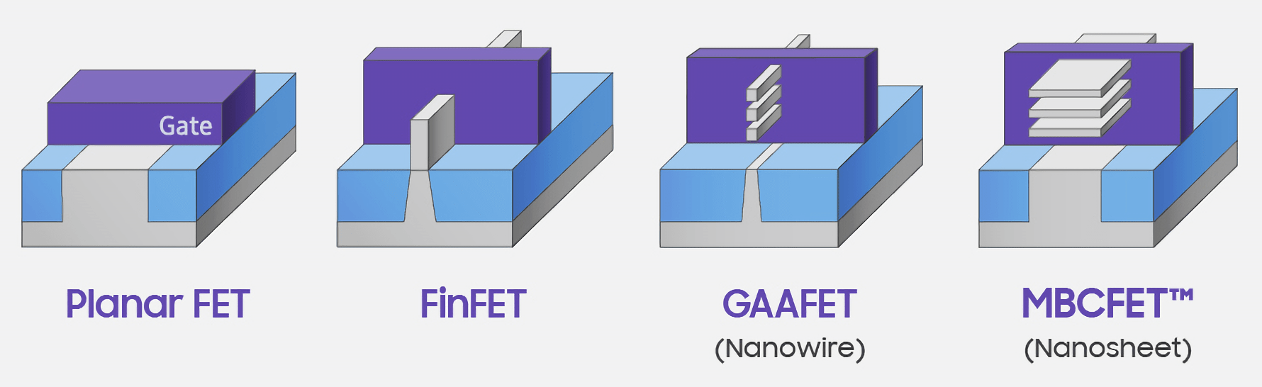
As AnandTech recounts, TSMC’s 3nm N3 node will continue to utilize FinFET transistors rather than switching to something like a Gate-All-Around (GAA) design a la Samsung. Compared to N5, N3 is expected to improve performance by 10-15 percent and boost power efficiency by as much as 25-30 percent.

Also in the cards is a 1.7x improvement in logic density.

Per TSMC’s roadmap, N3 will enter risk production in 2021 ahead of going into volume production sometime during the second half of 2022.

In the interim, consumers have a couple of other nodes to look forward to.

The aforementioned N5 node is expected to be used in Apple’s iPhone 12 family due out perhaps as early as next month. An optimization of this node, N5P, is also in the works that’ll boost performance and power efficiency by five and 10 percent, respectively, over the standard N5 node. N4 was also briefly mentioned, with risk production set to start in Q421 ahead of volume production the following year.

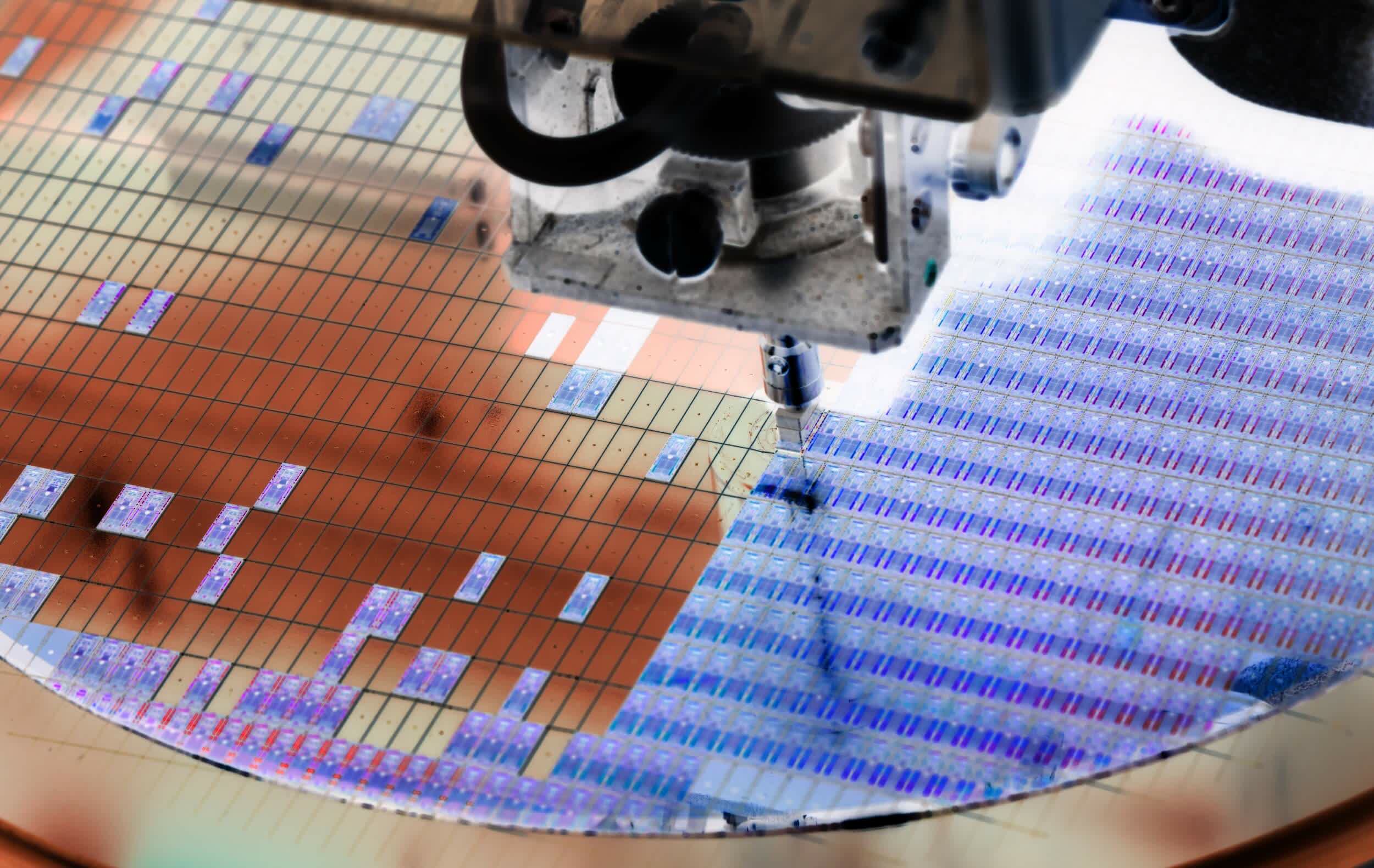
Image credit: Marco photo

Permalink to story.

 
It's absolutely amazing - I remember folks saying this stuff was practically impossible - with quantum tunneling - heat resistance etc etc . Add in the future when AI can absolutely slaughter us in chip design- interesting times
 
Interesting that n4 and n5 are going into risk production and should be coming to market about the same time. Will companies be able to adapt to n4 from n5 with few changes to their current designs?

*chuckles to self about current designs being an unintentional pun
 
It's absolutely amazing - I remember folks saying this stuff was practically impossible - with quantum tunneling - heat resistance etc etc . Add in the future when AI can absolutely slaughter us in chip design- interesting times

It is amazing but 3nm is the hard limit for silicone unless they find some new trick but at 3nm each transistor is only 15 atoms of silicone across. We will need to find a new material with smaller atoms or we need to start looking at other methods such as traffic via photons instead of electrons.
 
> "N3 is expected to improve performance by 10-15 percent and boost power efficiency by as much as 25-30 percent."

According to a slide I saw, N3 is expect to boost performance by 10-15% OR power efficiency by 30%. Not both simultaneously. It would be good to see a clarification on this.
 
It is amazing but 3nm is the hard limit for silicone unless they find some new trick but at 3nm each transistor is only 15 atoms of silicone across.
What TSMC is calling their 3nm node (N3) is really just pure marketing. The minimum feature size on their 7nm node is actually around triple that ... N3 is likely much the same.

And in any case, there are potential ways around the quantum effect gate tunneling problem that makes 3nm a potential roadblock.
Yeah... 3nm should not have 1.7x the density of 5nm. Even withing their naming scheme, calling it 4nm would be more accurate.
 
It is amazing but 3nm is the hard limit for silicone unless they find some new trick but at 3nm each transistor is only 15 atoms of silicone across. We will need to find a new material with smaller atoms or we need to start looking at other methods such as traffic via photons instead of electrons.
ROFL at the concept of soft squidgy transistors with a hard limit.
 
It is impressive how TSMC left everyone else in the dust...
I’m just wondering if this race has an impact on life expectancy of modern CPUs.
 
Well there is a hard limit
He was referring to the small typo:
It is amazing but 3nm is the hard limit for silicone unless they find some new trick but at 3nm each transistor is only 15 atoms of silicone across.
Silicone transistors are going to be quite a bit squiggier compared to silicon ones :)
 
It is impressive how TSMC left everyone else in the dust...
I’m just wondering if this race has an impact on life expectancy of modern CPUs.
Life expectancy is indeed something to consider. With circuit traces so close together at 3nm, it takes only the tiniest imperfection to get a little worse when subjected to repeated high termperatures, and blam! You have a useless malfuncrioning chip on your hands. We can expect reduce voltage to mitigate this somewhat, and cooling will continue to be very important.

Still, TSMC and Samsung are eating Intel's lunch, with AMD CPUs made by TSMC tagging along. When will Intel get out of its chip design doldrums?
 
> "N3 is expected to improve performance by 10-15 percent and boost power efficiency by as much as 25-30 percent."

According to a slide I saw, N3 is expect to boost performance by 10-15% OR power efficiency by 30%. Not both simultaneously. It would be good to see a clarification on this.
Why not simultaneously with ever lowered on-chip voltage?
 
Why not simultaneously with ever lowered on-chip voltage?

Because when you increase the number of transistors, your consumption increases. You can't go below a certain voltage, because some of the PN or NP joints will stop working at too low voltages.
 
Why not simultaneously with ever lowered on-chip voltage?
New nodes are usually quantified by giving two data points: power reduction at constant performance, and performance enhancement at constant power.

Graph those two points on an X-Y grid, connect them with a line (a curve, actually, but a line gets you close) and a chip designer can optimize for either maximum, or any point in between.
 
Back