
First look: Light, not silicon, may define the next leap in computing power. That's the bet Austin-based startup Neurophos is making as it challenges the idea that Moore's Law still governs the pace of performance progress. The company is developing a photonics-driven processor designed to do what decades of transistor scaling can no longer achieve: massive compute throughput without a proportional explosion in energy use.
The concept centers on an optical processing unit – a chip that performs calculations using light rather than electrons. Neurophos says its technology could reach 470 petaFLOPS of FP4/INT4 compute, roughly ten times the performance of Nvidia's latest Rubin GPUs, while drawing similar power. For an industry straining against the physical limits of silicon, it's an ambitious claim.
Neurophos founder and CEO Patrick Bowen describes the company's breakthrough as a shift in how computation itself is represented. Instead of manipulating charge across billions of transistor gates, the company's prototypes perform matrix multiplications optically, with beams of light passing through finely tuned metamaterials. Each microscopic modulator acts like an "optical transistor," directing photons to represent numeric weights in analog form.
"The equivalent devices built in standard silicon photonics are enormous – about two millimeters long," Bowen told The Register. "You can't pack enough of them to compete with digital CMOS." Neurophos says its micron-scale modulators are roughly 10,000 times smaller, small enough to be produced through standard CMOS foundry processes, eliminating one of the biggest roadblocks to commercial scale.
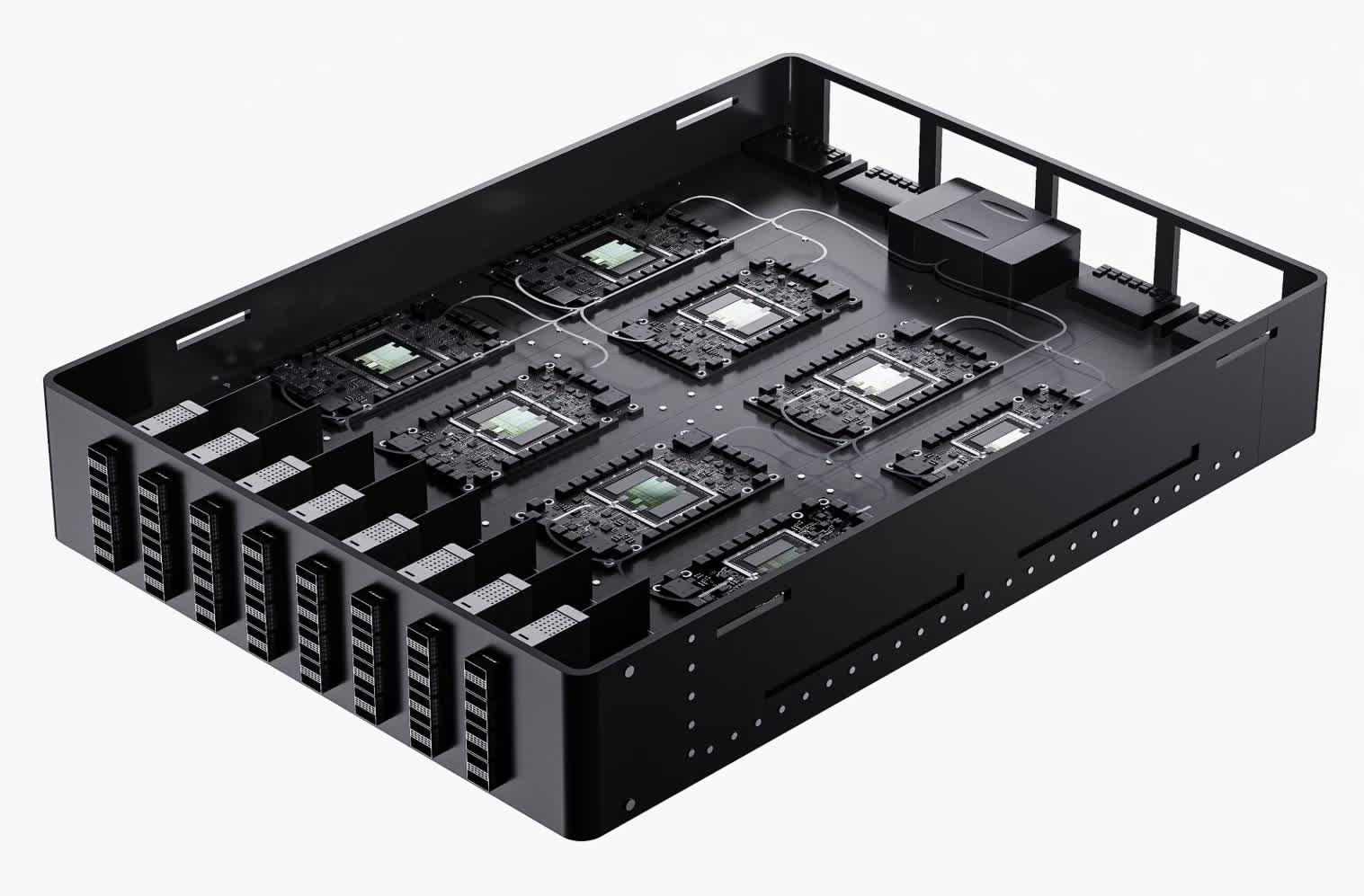
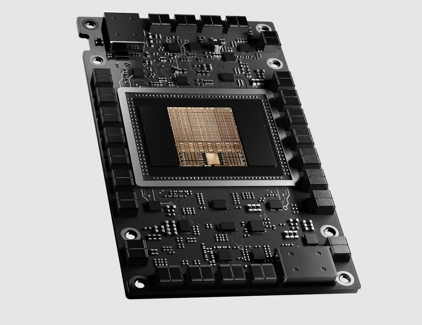
Instead of designing GPUs around an array of small compute tiles, each performing limited matrix math, Neurophos' approach is based on a single enormous photonic tensor core: a 1,000-by-1,000 processing element matrix that forms the computational heart of the OPU. That's roughly fifteen times larger than the 256-by-256 cores used in most AI accelerators.
Though only one such tensor core fits on the company's first-generation die – occupying about 25 square millimeters – it runs incredibly fast. Neurophos says this optical matrix operates at around 56 gigahertz, orders of magnitude beyond typical GPU clock speeds that rarely exceed single-digits.
Crucially, the optical core itself consumes little power; most of the chip's energy goes into the opto-electrical conversions needed to translate data between photons and electrons.
To sustain that 56 GHz core, Neurophos' engineers had to build a dense supporting architecture of vector units and SRAM. These elements feed data fast enough to keep the optical core busy – a major challenge given the difference between optical speed and electronic memory latency. The startup's engineering team refers to this supporting logic as "the boondoggle" that makes the core viable.
The first chip, the Tulkas T100, features a dual-reticle design and 768 GB of high-bandwidth memory. Operating under load, it's projected to deliver 470 petaOPS at 1 – 2 kilowatts of power. Though still theoretical, the numbers suggest compute densities that could redefine inference acceleration if the chip performs as modeled.
Neurophos expects that early use cases will focus on AI inference prefill – the compute-intensive phase of large-language-model processing in which input tokens are processed before text generation begins. It's a workload Nvidia itself has begun optimizing with the Rubin CPX accelerator. Bowen envisions linking one rack of 256 Tulkas chips with something like Nvidia's NVL576 rack, complementing rather than competing directly with existing GPU architectures.
Mass production is several years away. Neurophos doesn't expect its OPU to ship before 2028, and volumes will be limited – thousands of chips rather than tens of thousands. In the meantime, the company is building a proof-of-concept chip to test its claims of power and compute density.
Neurophos recently closed a $110 million Series A funding round led by Gates Frontier, the investment arm of Bill Gates, with participation from Microsoft's venture fund and other investors. The funding will support fabrication of the proof-of-concept system and early integration testing with standard optical interconnects.