Forward-looking: For years, ASML has been synonymous with one technology: extreme ultraviolet lithography, or EUV – the painstakingly engineered process that makes today's most advanced chips possible. But as AI pushes semiconductors to new physical and economic limits, the Dutch company is preparing to expand beyond lithography itself. The future of AI hardware may depend not just on etching smaller transistors, but on rethinking how chips are built, packaged, and scaled.
The company's next moves include building machines for advanced chip packaging and exploring ways to produce even larger silicon dies, shifting ASML from its narrow role as the world's sole EUV supplier into a broader supplier of AI-era chipmaking tools. CTO Marco Pieters, who took over in October 2025 after a 40-year tenure by Martin van den Brink, described the effort as a long-term strategy rather than a short-term adjustment.
"We look not just for the next five years, we look at the next 10, maybe 15," he said in an interview with Reuters.
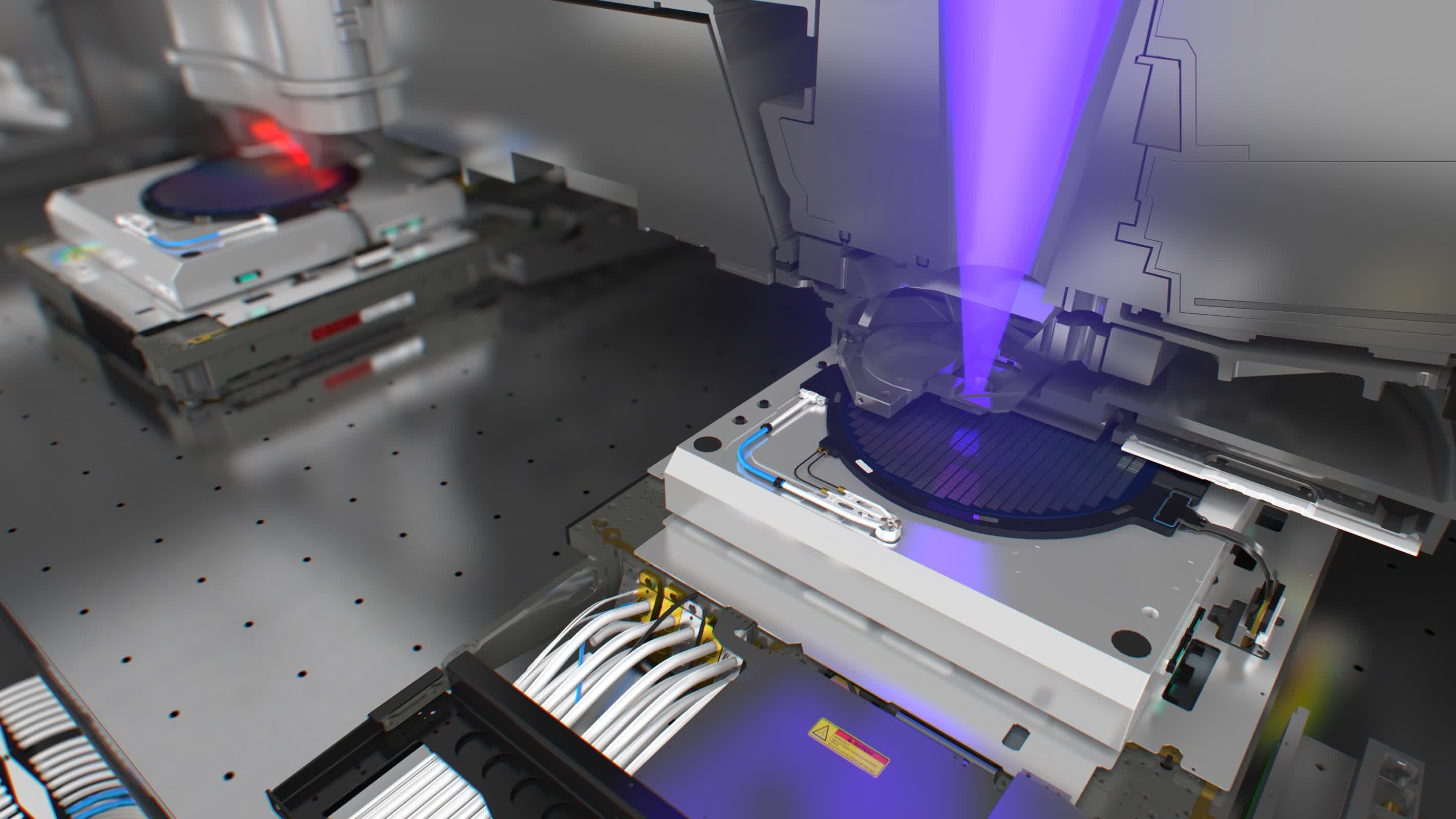
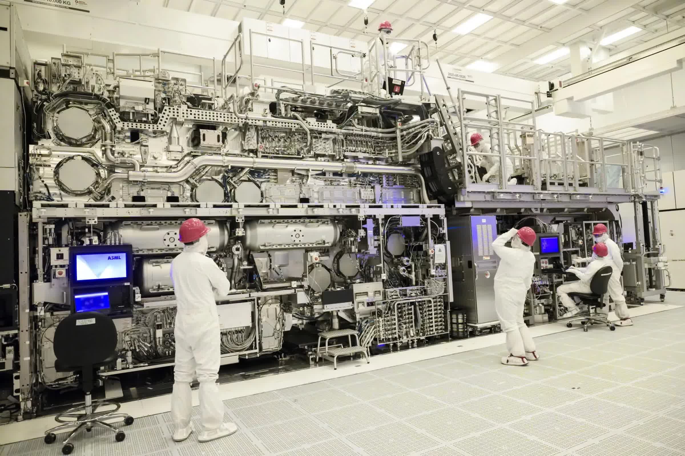
ASML's EUV machines have been the foundation for TSMC and Intel as they push chip features well below 5 nanometers. After more than a decade of research and billions in development, ASML's second-generation EUV tools are near production, with a third in early research.
But the limits of this success are increasingly clear. EUV tools currently print areas roughly the size of a postage stamp. That boundary constrains chip size and speed. Engineers at ASML are now exploring optical and mechanical redesigns to expand that printable field, potentially enabling the creation of physically larger, more powerful chips.
What once seemed a routine manufacturing step: connecting chips to circuit boards – is now one of the semiconductor industry's most critical bottlenecks. As chipmakers like Nvidia, AMD, and memory manufacturer SK Hynix build ever-larger devices, they've begun layering chips vertically and horizontally, creating "skyscraper" architectures linked by microscopic bonds.
Advanced packaging integrates multiple silicon dies into a single, unified component that communicates faster and consumes less power than a single monolithic chip. Companies like TSMC already use sophisticated packaging technologies to build Nvidia's flagship AI accelerators. For ASML, the shift presents both a challenge and a business opportunity.
AI isn't just driving demand for ASML's customers, it's also reshaping how ASML builds and operates its own machines.
Pieters said the company is now designing manufacturing equipment specifically for these multi-die systems – tools capable of handling the delicate alignment and bonding required for 3D packaging. "We're researching to what extent we can participate in it, or what we can add to that part of the business," he said.
AI isn't just driving demand for ASML's customers, it's also reshaping how ASML builds and operates its own machines. Pieters, whose background is rooted in ASML's software divisions, said AI will be used to accelerate control algorithms and inspection processes within the company's future lithography and packaging tools.
Those systems already collect vast streams of high-resolution optical data during every wafer pass. Improving their analysis with machine learning could reduce downtime and increase yield.
The first product signaling this diversification arrived last year: the XT:260 scanner, designed for advanced memory chips used in AI applications. Engineers are now investigating additional systems that could extend those capabilities to even more complex logic and stacking operations.
To focus more heavily on engineering, ASML streamlined its technology division and Christophe Fouquet – CEO since 2024 – has aligned the corporate roadmap around expansion beyond EUV lithography.
The confluence of optics, motion systems, and silicon handling gives ASML a technical foundation few can match. Pieters said this expertise will underpin new product lines for at least the next decade. He said the planned scanners, bonding gear, and control systems are meant to complement ASML's long-standing lithography products, adding: "It will co-exist next to what we've been doing for the last 40 years."