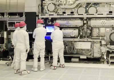
Semiconductor articles

intel apple nvidia tsmc rumor leak intel 18a

Intel may scrap 18A node in favor of 14A to attract Apple and Nvidia

New CEO distances company from Gelsinger's 18A legacy, could lead to billion-dollar write-off
TL;DR: Intel CEO Lip-Bu Tan is reportedly considering scrapping the company's 18A manufacturing process for external foundry customers. Instead, Tan wants Team Blue to focus on the newer and more efficient 14A node in hopes of securing major clients like Apple and Nvidia away from TSMC.
trump tsmc semiconductor tariffs donald trump wafer

TSMC's 2nm wafer prices hit $30,000 as SRAM yields reportedly hit 90%

Apple, Intel, Nvidia, and others line up for next-gen chips
In context: TSMC has steadily raised the prices of its most advanced semiconductor process nodes over the past several years – so much so that one analysis suggests the cost per transistor hasn't decreased in over a decade. Further price hikes, driven by tariffs and rising development costs, are reinforcing the notion that Moore's Law is truly dead.
intel cpu intel core semiconductor opinion with video

Intel doubles down on foundry ambitions, unveils 18A and 14A process enhancements

New CEO means to woo foundry clients
In context: Intel's recent challenges are undoubtedly familiar to anyone who has paid even the slightest attention to the semiconductor market. These issues were a key reason the company recently appointed semiconductor industry veteran Lip-Bu Tan as its new CEO. Some even speculated that Intel might spin off its chip-making foundry business.
chip enterprise ai design industry opinion automation chipmakers cadence synopsys

AI is reshaping chip design tools, and the results are impossible to ignore

Why it matters: As powerful as AI may be, many industries are still struggling to find clear-cut applications that make a measurable, demonstrable difference. Thankfully, that is not the case when it comes to chip design software. In fact, since their introduction just a few years ago, AI-powered features have become a mainstay of EDA (Electronic Design Automation) tools from companies such as Cadence and Synopsys.
researchers 3d chip

Researchers use lasers and metalenses to align 3D chips with atomic precision

Forward-looking: Researchers at the University of Massachusetts Amherst have developed a laser-based technique to align 3D semiconductor chips, potentially overcoming a longstanding challenge in chip manufacturing. The method employs concentric metalenses to generate holograms that reveal misalignment between chip layers at a much smaller scale than previously possible.