The takeaway: Elon Musk is betting that building his own chips is the only way to keep pace with the computing demands of his ambitions in robotics, autonomous driving, and space. This weekend, he put a location and a rough blueprint behind that bet, triggering fresh questions about whether even his track record of taking on hard engineering problems will be enough to overcome the realities of modern chipmaking.
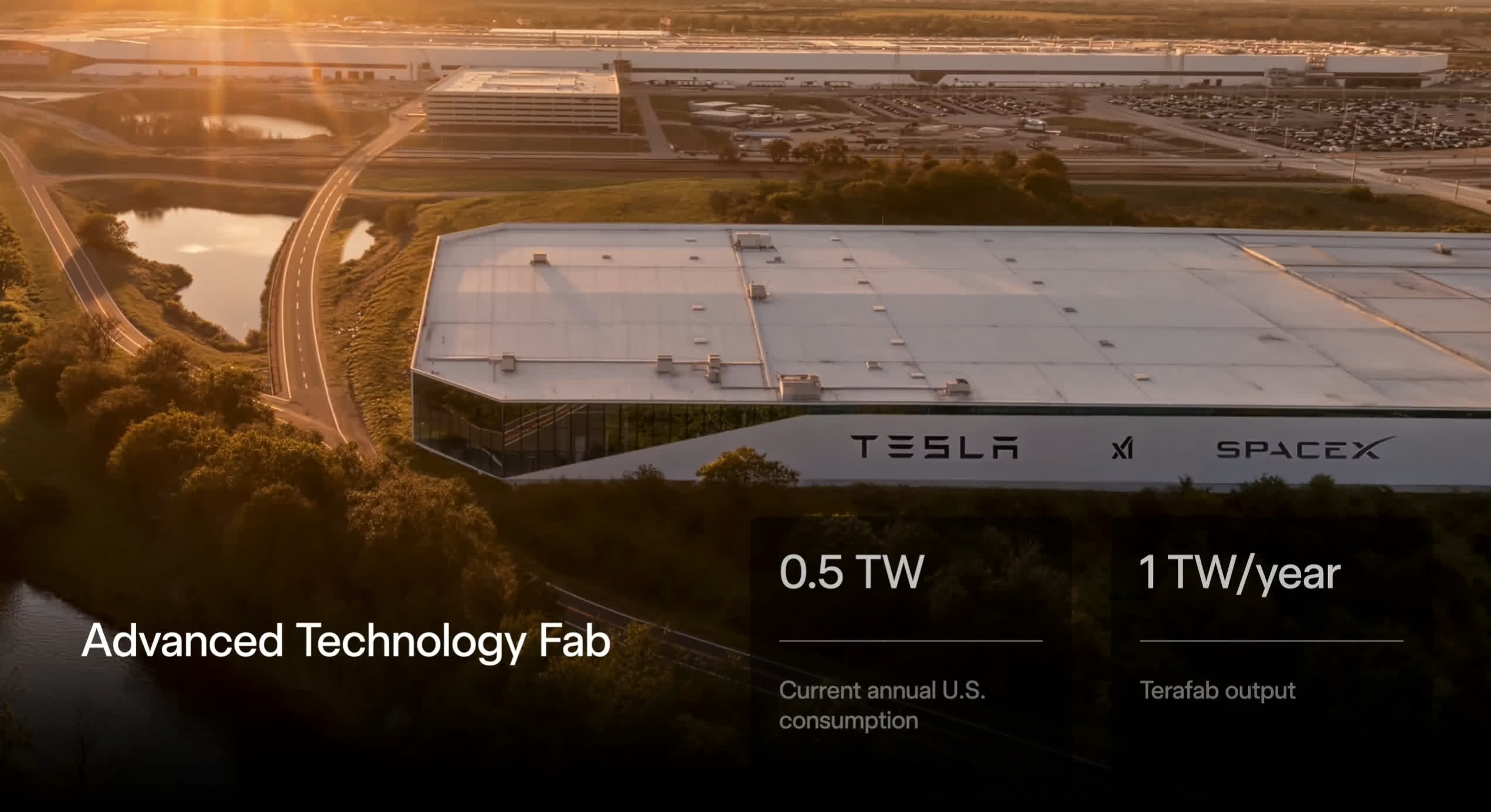
Speaking at an event in downtown Austin, Musk said a new Terafab project will be jointly run by Tesla and SpaceX and anchored by what he called an "advanced technology fab" in the city that can make and test "chips of any kind."
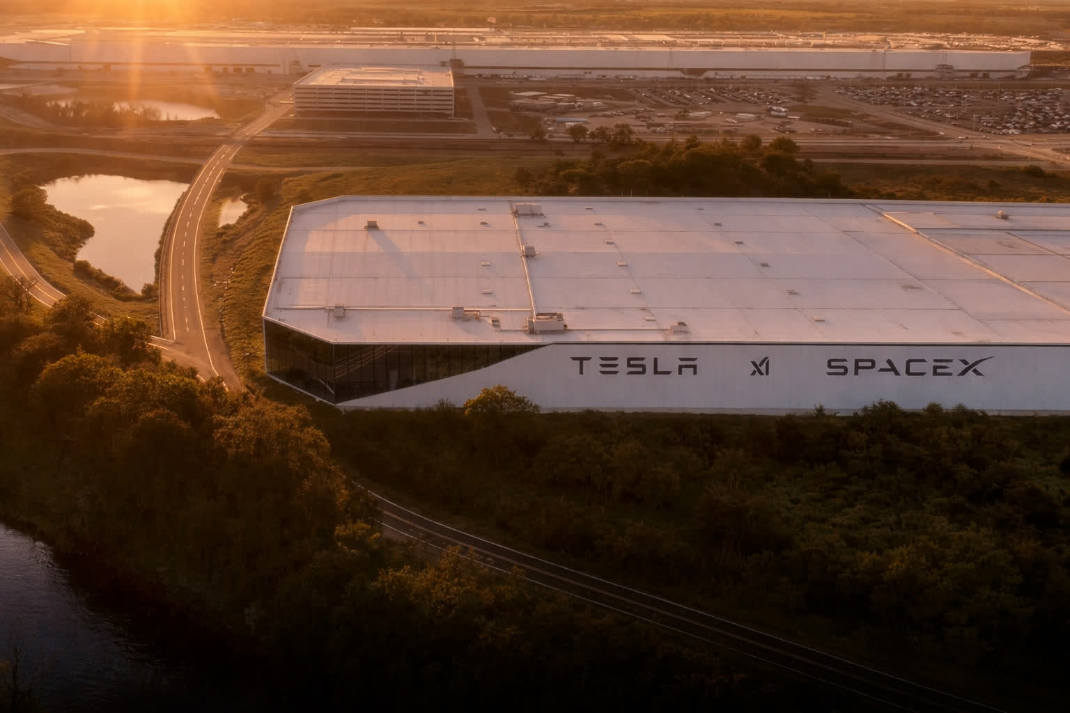
Musk revealed that the facility would be located near Tesla's Austin headquarters and gigafactory, according to a site image he displayed during the presentation. He previously said the plant would target 2-nanometer process technology, putting it in competition with the world's most advanced foundries.
– Tesla (@Tesla) March 22, 2026
The initiative is Musk's response to what he describes as a looming shortage of the specialized chips needed to power Tesla's planned robotaxis, humanoid robots, and the data centers that will train and run their AI models. On a January earnings call, he warned investors that production from key suppliers would fall far short of Tesla's requirements as those programs scale. "This is definitely going to be sort of a controversial thing, but I think Tesla needs to build a Terafab," he said.
Musk has outlined the project in terms of raw computing power as much as chip counts. He previously said the ultimate goal is to support roughly a terawatt of computing per year.
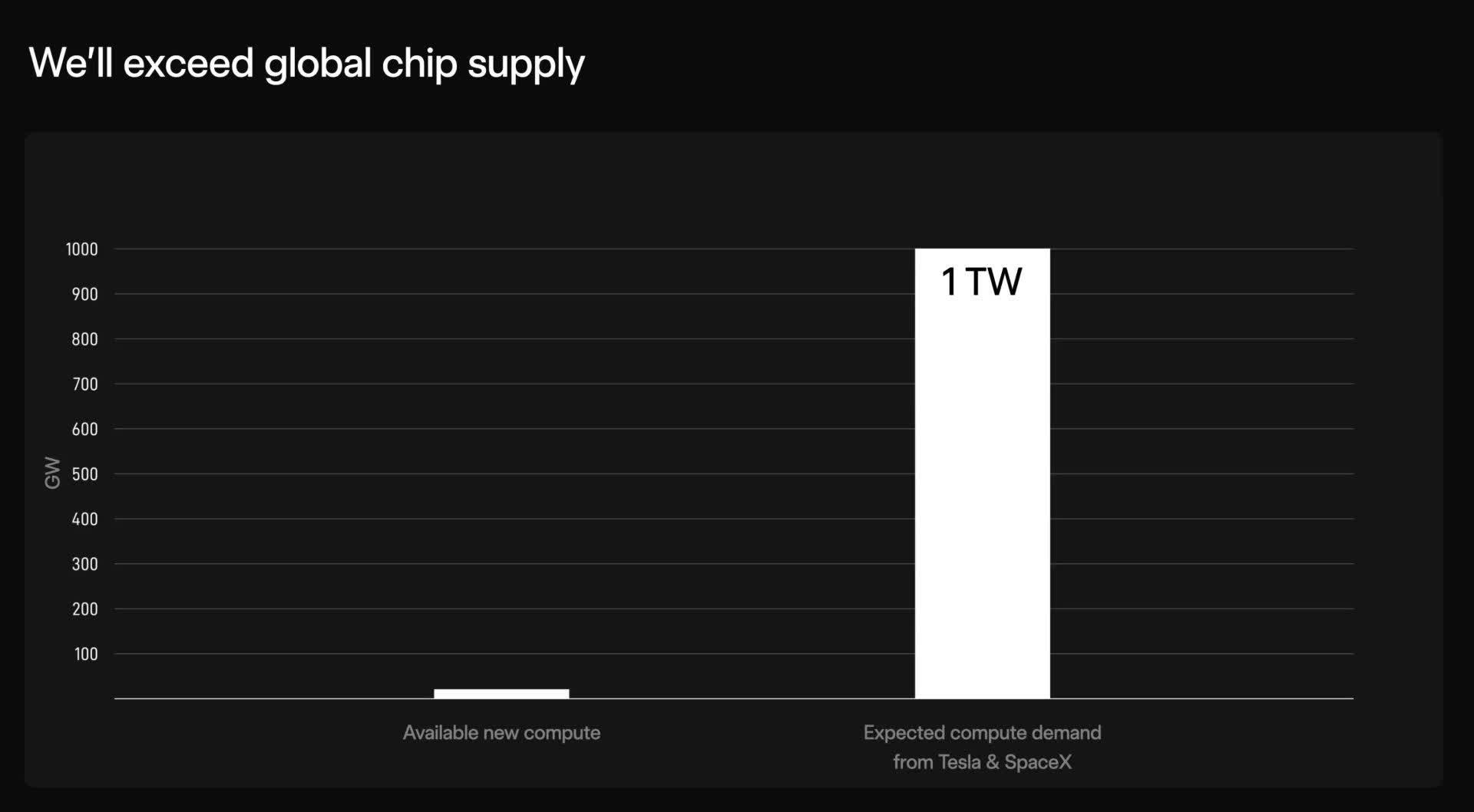
In Austin, he described plans to produce chips that could back 100 to 200 gigawatts of computing power annually on Earth and reach a terawatt for space-based systems.
At Tesla's annual shareholder meeting last November, the billionaire estimated that Terafab would start by producing about 100,000 silicon wafers a month and could eventually scale to 1 million wafers monthly. More recently, Musk said Tesla will begin with a smaller fab and then expand, but the core concept remains a very large, vertically integrated plant in the United States that handles both logic and memory chips.
For now, the plan exists mainly on paper and in early hiring. Tesla has posted a role for a semiconductor infrastructure manager based in Austin to oversee factory design and construction.
Musk said the first phase will be a fully equipped "advanced technology fab" capable of making and testing a wide range of devices, but he did not disclose when construction would begin, when tools would arrive, or when volume production might start. He also hasn't detailed how the facility would coordinate Tesla's automotive and robotics needs with SpaceX's space computing demands, beyond noting that the two companies will run it together.
Industry specialists say Musk is targeting one of the most challenging areas of modern manufacturing. For instance, Stacy Rasgon, managing director and senior semiconductor analyst at Bernstein, told Business Insider that getting access to those ASML machines represents a fundamental choke point for any new entrant. "If you're a brand new customer, you're probably waiting a couple of years before getting your hand on one of those," he said.
Rasgon also pointed to the way the industry usually separates different parts of the manufacturing chain, with logic, memory and packaging often handled in different plants or even by different companies. Musk's vision of combining those activities into a single facility further raises the integration challenge, because each product type follows distinct process steps and economics.
– Elon Musk (@elonmusk) March 14, 2026
Despite Musk's history of defying skeptics at Tesla and SpaceX, Rasgon said he believes Terafab may be "harder than sending rockets to Mars."
Analysts at other firms share concerns about cost and execution. In a note to clients, Morgan Stanley analysts led by Andrew Percoco cited Micron's memory fab in Boise – which began construction in late 2022 and is not expected to ship chips until mid-2027 – as a reminder of how long US semiconductor projects take to move from groundbreaking to output.
They estimated that a factory capable of producing 100,000 wafers of cutting-edge logic chips a month could require as much as $45 billion in investment. UBS analysts have separately put the cost of reaching Musk's initial 100,000-wafer target at around $30 billion. Morgan Stanley described Musk's plan as a "Herculean task" even allowing for his past success with challenging engineering projects.
How Tesla would finance such an effort remains open. Ben Kallo, a senior research analyst at Baird, said that investors are likely to press for details on funding, especially since Musk has also talked about building roughly 100 gigawatts of solar manufacturing capacity.
Beyond capital and equipment, talent may be another limiting factor. The semiconductor industry already faces a shortage of experienced engineers and technicians, and leading firms have had to import expertise to get new fabs running.
TSMC, for example, has flown workers from Taiwan to Arizona and sent US employees to its home facilities for months of training as part of its US expansion. Rasgon said the specialized knowledge required to run cutting-edge fabs will make recruiting critical for Tesla's plans. "These guys don't grow on trees," he said.
Musk has not set a firm deadline for when Terafab will be built or when it might start shipping products, but he told investors in January that the goal is to remove what he sees as a "probable constraint" on Tesla's growth over the next three to four years. In a post on X days before the Austin event, he wrote that "Terafab Project launches in 7 days," signaling that, at least in his view, the clock on that constraint has already started.