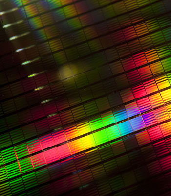
Micron Technology has announced what it claims is the industry's densest 128Gbit NAND flash memory device. With die area of only 146 square millimeters, the chip is made using a 20nm fabrication process and is based on triple-level-cell flash technology.
According to Micron, the new chip measures 12mm x 12mm and is roughly 25% smaller than a similar capacity 20nm multi-level-cell NAND device.
Triple-level-cell (TLC) flash technology is similar to single-level-cell (SLC) and multi-level-cell (MLC). All three consist of similar transistors, the difference is that they store a different amount of bits per cell. SLC only stores one, whereas MLC stores two and TLC stores three. Adding more bits per cell leads to higher storage density but it also reduces endurance while increasing program, erase and read latencies. In other words this is why pricier SLC NAND is mostly limited to business applications while MLC and TLC flash chips are found on consumer products.
Micron isn't targeting their TLC NAND at SSDs but rather at the cost-competitive removable storage market (flash cards and USB drives), which is projected to consume 35% of total NAND gigabytes in calendar 2013.
But TLC flash chips are indeed making their way into SSDs and will be an important factor in bringing prices further down. Last year, Samsung introduced the first commercially available TLC NAND based SSD in the form of the Samsung 840 (a cheaper version of the Pro variant we reviewed). Even with the performance implications of TLC, many reviewers have found Samsung's 840 SSD to be faster than previous generation MLC based alternatives while offering similar or higher endurance as well. That's encouraging for the technology but also speaks about Samsung's skill when comes to designing a controller, firmware, and NAND chips themselves.
