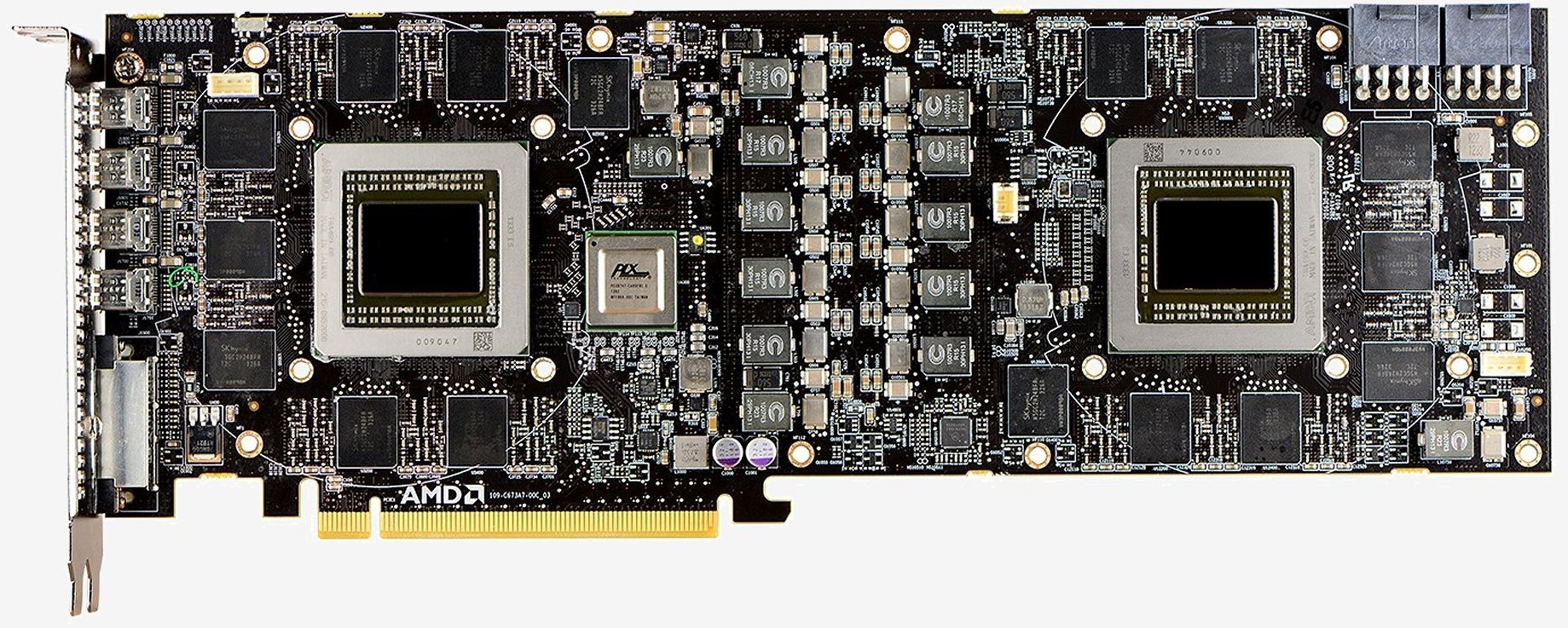
We first caught wind of an upcoming dual-GPU Hawaii graphics card this time last month when AMD teased us with its top-secret "Two is Better Than One" campaign. Although AMD didn't actually reveal anything, it was clearly planning a successor to the Radeon HD 7990, which is essentially two Tahiti dies on a single board, or in other words a pair of slightly underclocked Radeon HD 7970 GHz Edition GPUs.
Back when we tested the 7990 in April 2013, it was a formidable rival for the GeForce GTX Titan. The biggest problem the card faced was AMD's frame latency performance, which was quite poor at the time, especially compared to a single-GPU solution like the Titan. The 7990 also suffered from enormous power consumption figures compared to the Titan, as we found it pulled almost 40% more power.
Nonetheless, putting a pair of 28nm GPUs – each containing 4.3 billion transistors – onto a single PCB measuring just 12in (30cm) long was an impressive feat of engineering. In fact, this is what made the single-GPU flagship R9 290X even more impressive last October. Although it was built using the same 28nm process, Hawaii XT packs 6.2 billion transistors, blowing the die size up to 438mm2 from 352mm2.
That expansion allows for 38% more SPUs than the HD 7970 GHz Edition, though it also make the 290X 20% more power hungry, giving it a TDP of roughly 300 watts! The card's enormous power draw resulted in a huge thermal output – so much so that R9 290Xs often throttled just to maintain stability. Realizing this, we weren't sure if AMD was seriously considering two Hawaii XT GPUs on a single PCB.
Apparently so, as today marks the arrival of the Radeon R9 295X2, the most extreme graphics cards we have ever seen. It's hard not to be impressed when specs like 12.4 billion transistors, 5632 stream processors and 11.5 TFLOPS of compute power are being thrown around, not to mention the card's 8GB of GDDR5 memory and dual 512-bit memory bus, which provide a total memory bandwidth of 640GB/s.
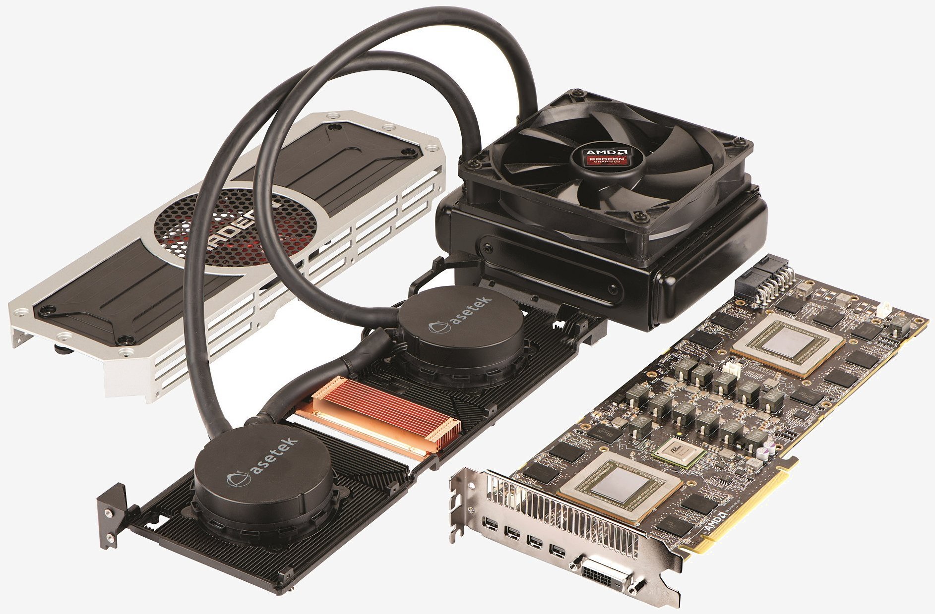
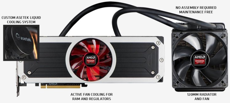
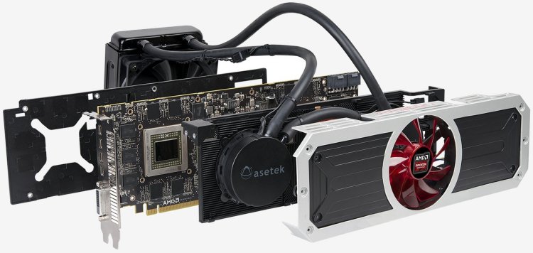
AMD says that this graphics card is "not for the faint of heart" and that users should "handle with extreme caution." The company faced two main challenges in developing the R9 295X2: keeping it cool and keeping it fed. The former is tackled by a dual-block closed-loop liquid cooler made by Asetek, and with a 500-watt thermal design power, the latter is more like a rite of passage for your power supply.
Meet the R9 295X2
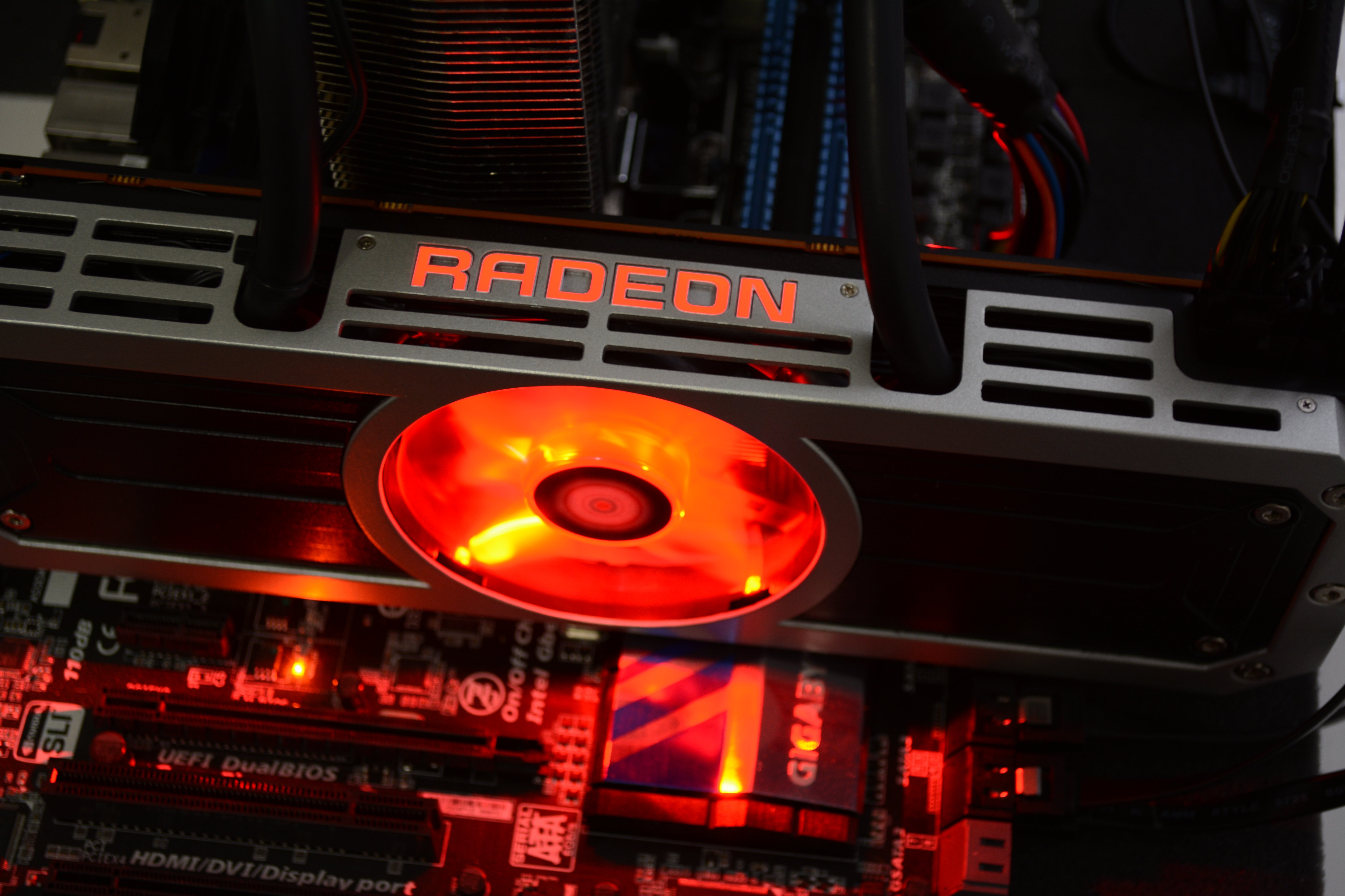
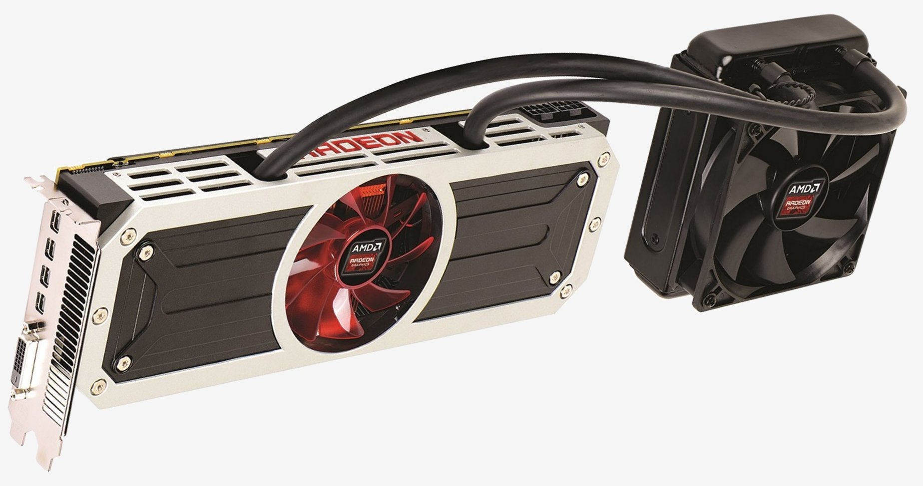
Measuring a motherboard-bending 12in (30cm) long, the R9 295X2 is roughly 3cm longer than the R9 290X and it's a very heavy graphics card featuring a full metal construction including the backplate and fan shroud.
Speaking of the fan, we never expected such an insane graphics card would be cooled via a single fan and, well, it's not. In fact the fan is used only to cool the GDDR5 memory and power regulators.
The GPUs are cooled using a pair of Asetek liquid cooling blocks, but we will get to them shortly. For now let's check out the cards specifications...
The card's GPU core is clocked at up to 1018MHz and it's the same deal as the R9 290X... if the thermal load reaches 95℃ then the clock speed will be throttled down to keep temperatures in check. AMD hasn't said how low the GPUs will underclock so we will have to look at this when testing.
| Radeon R9 295X2 | Radeon R9 290X | Radeon R9 290 | |
| Process | 28nm | 28nm | 28nm |
| Transistors | 12.4B | 6.2B | 6.2B |
| Engine Clock | Up to 1.02 GHz | Up to 1 GHz | Up to 947 MHz |
| Primitive Rate | 8 prim /clk | 4 prim /clk | 4 prim /clk |
| Stream Processors | 5,632 | 2,816 | 2,560 |
| Compute Performance | Up to 11.5 TFLOPS | 5.6 TFLOPS | 4.9 TFLOPS |
| Texture Units | 352 | 176 | 160 |
| Texture Fillrate | Up to 358.3 GT/s | Up to 176.00 GT/s | 152.00 GT/s |
| ROPs | 128 | 64 | 64 |
| Pixel Fillrate | Up to 130.3 GP/s | Up to 64.0 GP/s | Up to 64.0 GP/s |
| Z/Stencil | 512 | 256 | 256 |
| Memory Bit-Interface | 2 x 512-bit | 512-bit | 512-bit |
| Memory Type | 8GB GDDR5 | 4GB GDDR5 | 4GB GDDR5 |
| Data Rate | Up to 5.0 Gbps | Up to 5.0 Gbps | Up to 5.0 Gbps |
| Memory Bandwidth | Up to 640.0 GB/s | Up to 320.0 GB/s | Up to 320.0 GB/s |
As is the case with the R9 290X and R9 290, the R9 295X2's GDDR5 memory is clocked at 1250MHz for 5.0Gbps of bandwidth. Combine that with the 512-bit memory bus and you have a graphics card that is feeding a theoretical peak bandwidth of 320GB/s to each GPU. That's 10% more than the HD 7990.
Moreover, whereas the HD 7990 came loaded with a measly 6GB of memory the R9 290X2 has been upgraded with 8GB of memory (4GB per GPU). This sounds like overkill, but AMD is targeting Ultra HD displays with this graphics card.
We've found when using multi-monitor setups at extreme resolutions in the past that the larger buffer of AMD cards provide a significant advantage over Nvidia's, which were limited to 2GB for the most part (think GeForce GTX 690). That said, the new GTX Titan and GTX 780 Ti have a 6GB memory buffer for a single GPU.
The cores on the R9 295X2 are the same as the single-GPU R9 290X version. Each GPU carries 2816 SPUs, 176 TAUs and 64 ROPs, so in a sense you can double those figures for the R9 295X2.
Connecting the two GPUs is the PEX bridge from PLX Technologies, which is the same method employed by all previous AMD dual-GPU graphics cards. However, the R9 295X2 gets the latest 3.0 PEX8747 bridge which boasts 48 PCI Express 3.0 lanes for 96GB/s of inter-GPU bandwidth.
To feed the card enough power, AMD includes dual 8-pin PCI Express connectors – the same setup you'll find on the HD 7990 and even the 6990 before it. When it comes to feeding the R9 295X2 enough power safely, things become a little more complicated as we will explain shortly.
Naturally, the R9 295X2 supports Quadfire (Crossfire), though like the R9 290X there isn't a bridge connector as communication between the two cards is done via the PCI Express bus. The only other connectors are on the I/O panel. Our AMD reference sample has a dual DL-DVI connector and four mini-DisplayPort 1.2 sockets which allows support for five simultaneous monitors right out of the box.
