AMD's Vega GPU is just around the corner, and it's a much larger architectural upgrade than we expected. AMD divulged a bunch of new details about Vega at their Tech Summit last month, and while we don't have any graphics card information or specifications at this stage, AMD fans have a lot to be excited about in the coming months.
For much of 2016, it was assumed that Vega was simply a larger version of Polaris with more compute units, complete with High Bandwidth Memory. It's now clear that Vega contains significant architectural improvements that will make AMD's next-generation graphics cards more powerful and more capable. In fact, it now seems that Polaris was a mere intermediary stepping stone as AMD transitioned their flagship GPUs from Fiji to Vega.
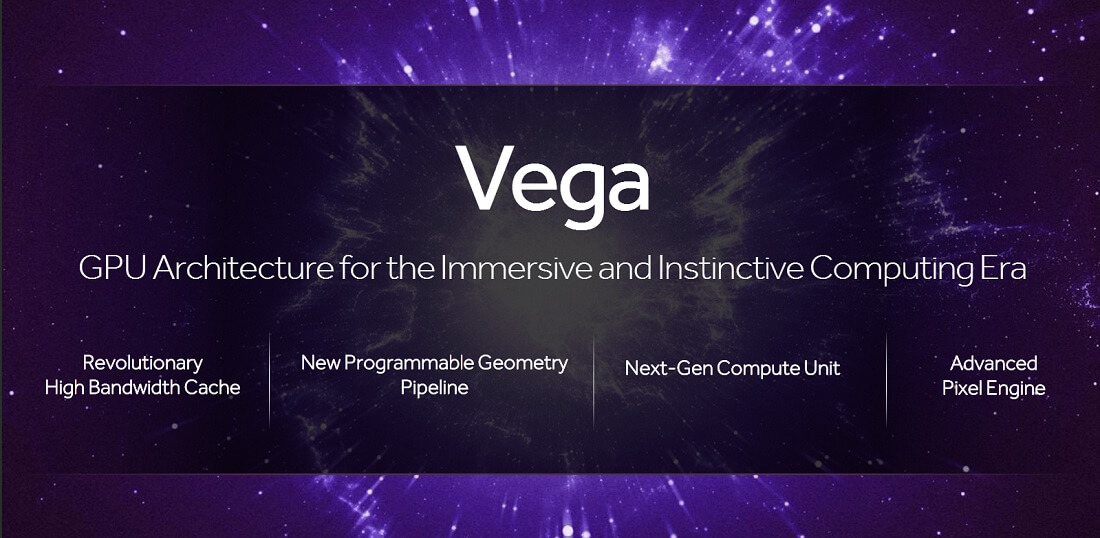
While Vega reportedly contains more than 200 new features, AMD spent time at their Tech Summit detailing the four most important changes. The biggest of these is a complete overhaul of their memory controller and structure, including the introduction of a High-Bandwidth Cache Controller (HBCC) and High-Bandwidth Cache.
One of the problems that AMD identified with their last-generation GPUs is that some applications need to access more data than is available in their VRAM. Compute applications in particular, along with professional rendering tools, are most susceptible to slowdowns due to these problems. Why? Well, traditionally if a GPU wants to access data outside its VRAM, it must first pause and transfer this data from system RAM or SSD/HDD storage into VRAM before any processing can take place.
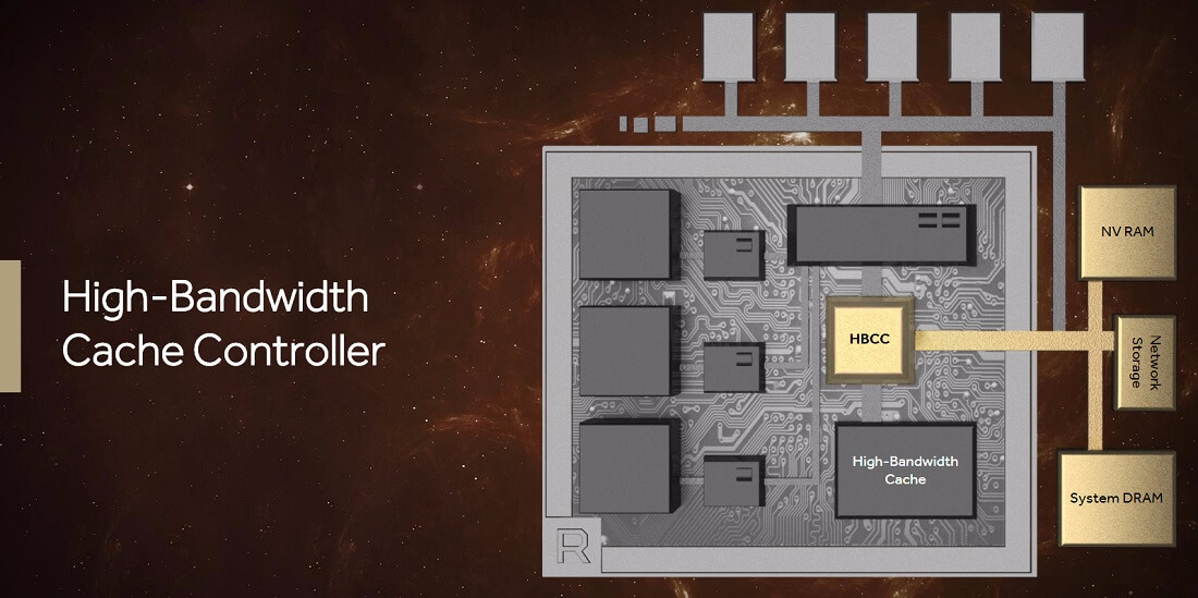
Vega changes this through the inclusion of a High-Bandwidth Cache Controller. AMD hasn't gone into detail on exactly how this controller works, but it seems as though it provides easier access to off-card storage like system DRAM, non-volatile RAM, and networked storage like SSDs and HDDs. Vega supports a virtual memory address space of 512 TB, which is far larger than any on-board VRAM solution, making it well suited to big data applications.
To demonstrate how useful the HBCC is, AMD showed off a scene being rendered on a Vega card using Radeon ProRender. This scene used hundreds of gigabytes of data, and was being rendered in real time, and even though the demonstration ran at only a few frames per second, AMD claimed that on previous cards it would have taken upwards of an hour to render each frame. Presumably these speed improvements have come from a drastic reduction in memory transfers per frame.
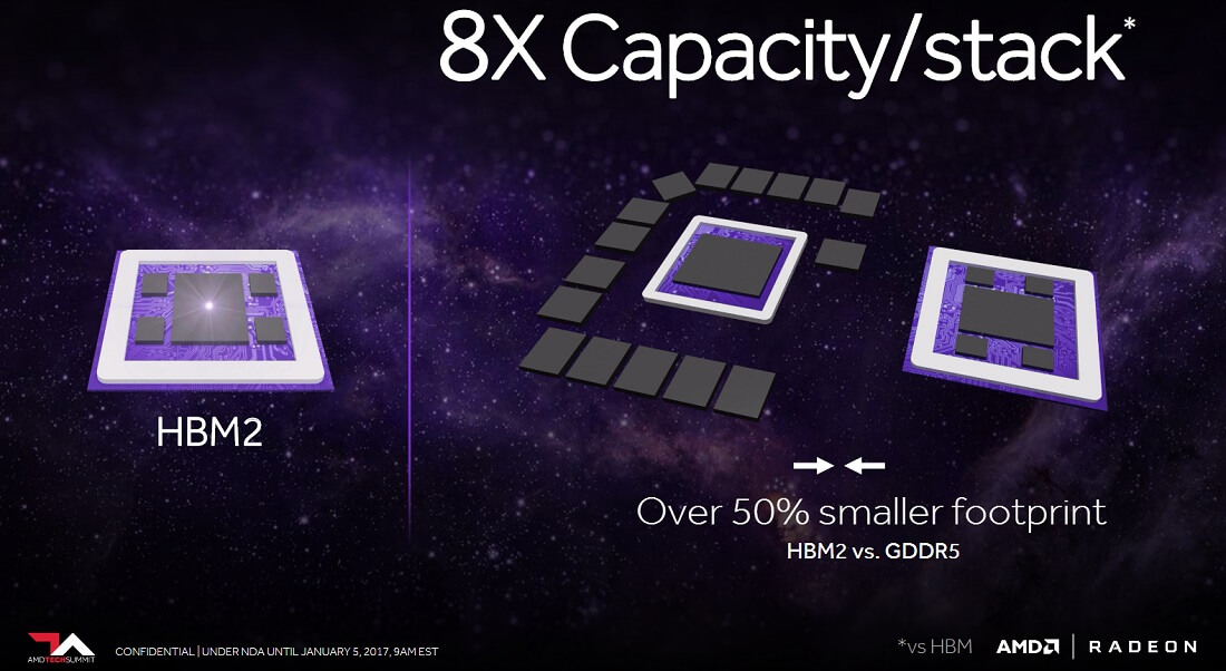
The HBCC also supports adaptive fine-grained data movement from external memory to Vega's on-die memory, which AMD is calling High-Bandwidth Cache. To be clear, High-Bandwidth Cache is simply a new name for VRAM, and in Vega this will be on-die HBM2. To speed up processing, the HBCC will dynamically shift the most scene- or compute-relevant data into Vega's HBM2.
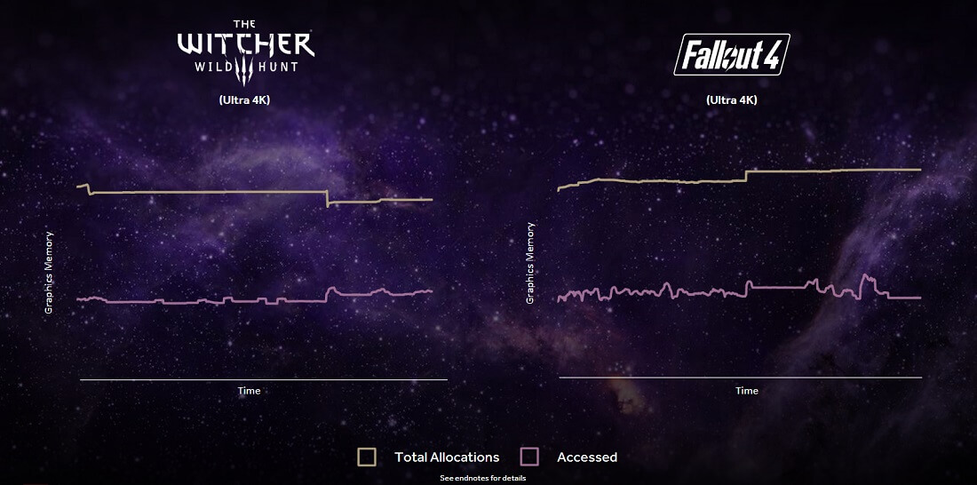
While the HBCC will have the biggest implications for compute workloads, AMD did suggest it will have some use in games. AMD showed a graph that illustrated how games allocate a lot of memory for any scene, but only access a fraction of it to render a frame. In the future, we could see games make use of HBCC-like technology by utilizing a lot more memory per frame while allocating more memory than the cache/VRAM can hold.
Vega comes with a next-generation compute unit called the Vega NCU. It supports 128 32-bit, 256 16-bit and 512 8-bit operations per clock; the latter two are particularly important for deep learning, and this is where Vega will boast significantly improved performance over older architectures. The NCU also supports flexible mixed-precision, and a configurable double precision rate.
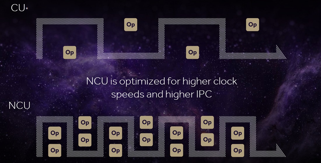
Aside from improvements to half and quarter precision performance, AMD claims the NCU is optimized for higher clock speeds and higher IPC, with an increased instruction buffer and an improved cache schedule.
Vega includes a new programmable geometry pipeline that offers over twice the peak throughput per clock. This pipeline is essentially a primitive shader, which sits alongside other shaders like the vertex shader and compute shader. It has the ability to launch threads at the same rate as the compute shader, and the pipeline in general offers improved load balancing, which is an issue console developers highlighted during their time working with previous GCN architectures.
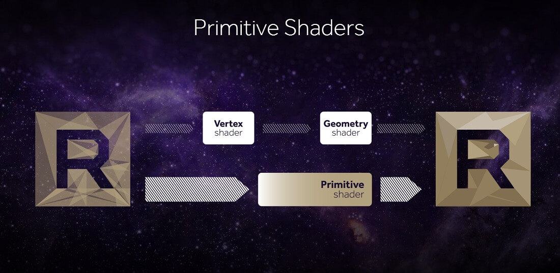
Developers will have to specifically target this new shader to get the most out of the Vega architecture, so it's not necessarily something we'll see utilized often, particularly for gaming workloads.
AMD has revamped the pixel engine in Vega as well, introducing a new rasterizer called the Draw Stream Binning Rasterizer. This rasterizer improves performance and power consumption by fetching only once for overlapping primitives, and shading only the pixels visible on screen. The pixel engine also now has access to L2 cache, which improves performance in deferred shading applications.
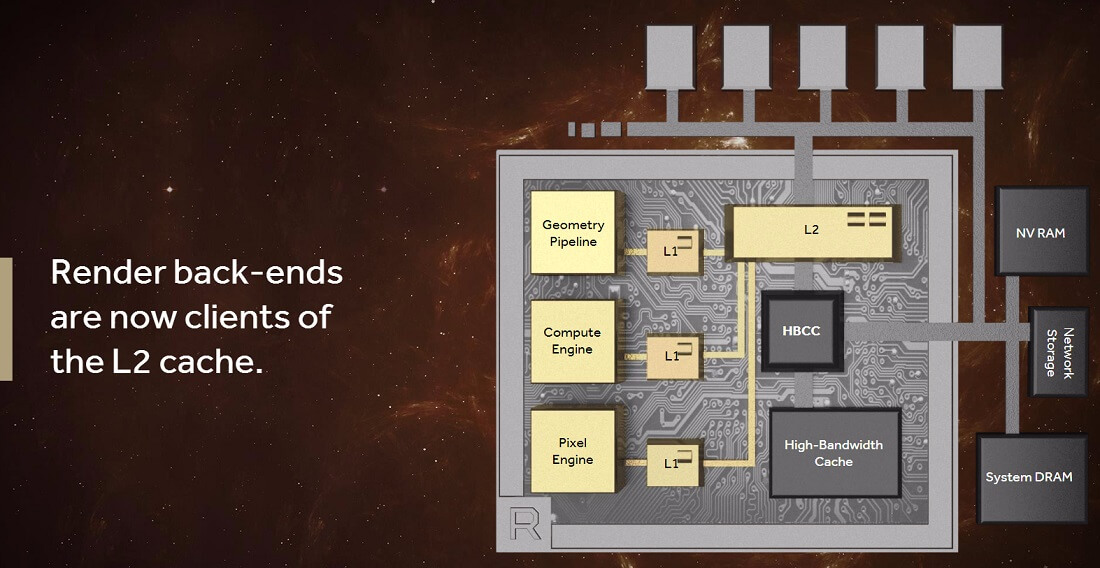
Basically, the pixel engine includes improvements that allow the GPU to work on stuff that actually needs to be worked on, while scheduling past work that doesn't contribute to a frame.
It could still be a little while before we see Vega graphics cards on the market, but AMD did have a working sample at their event, where they showed off Doom gameplay at 4K with ultra settings. In their demonstration, which was thrown together using beta drivers in a few weeks with little optimization, Vega achieved around 60 to 70 FPS, placing it in the same performance bracket as Nvidia's GeForce GTX 1080.
Vega sounds like a promising upgrade over AMD's past architectures, both for compute and gaming workloads. We'll have to wait a little while longer for AMD to reveal its consumer graphics card line-up and their corresponding specifications, but it's clear that AMD will have a high-performing flagship card in just a few months' time.
