
Why it matters: Talk to anybody in the semiconductor industry these days and all they seem to want to talk about is chiplets, the latest development in SoC (system on a chip) designs. The basic rationale behind chiplets is that several different developments are making the industry's traditional method of building increasingly larger chips less appealing, both technically and financially. So, instead of designing sophisticated, monolithic chips that incorporate all the important elements on a single silicon die, major semiconductor companies are designing products that break the larger designs into smaller pieces (hence "chiplets") and combine them in clever ways.
What makes chiplet design different from other SoC design methodologies that have existed for many years is that many of these new chiplet-based parts are putting together pieces that are made on different process technologies. So, for example, a chiplet design might link a 7 or 10 nm CPU with a 14 nm or 22nm I/O element over some type of high-speed internal interconnect.
The reason for making these kinds of changes gets to the very heart of some of the transformational developments now impacting the semiconductor business. First, as has been widely discussed, traditional Moore's Law advancements in shrinking transistor size have slowed down tremendously, making it difficult (and very expensive) to move all the elements inside a monolithic chip design down to smaller process geometries. Plus, even more importantly, it turns out that some important elements in today's chip designs, such as analog-based I/O and some memory technologies, actually perform worse (or simply the same, but at a significantly higher cost) in smaller-sized chips. Therefore, some semiconductor components are better off staying at larger process manufacturing sizes. In addition, the processing requirements for different types of workloads (such as AI acceleration) are expanding, leading to the need to combine even more types of processing technology onto a single component. Finally, there have been some important advancements in chip packaging and interconnect technologies that are making the process of building these multi-part chiplets more efficient.
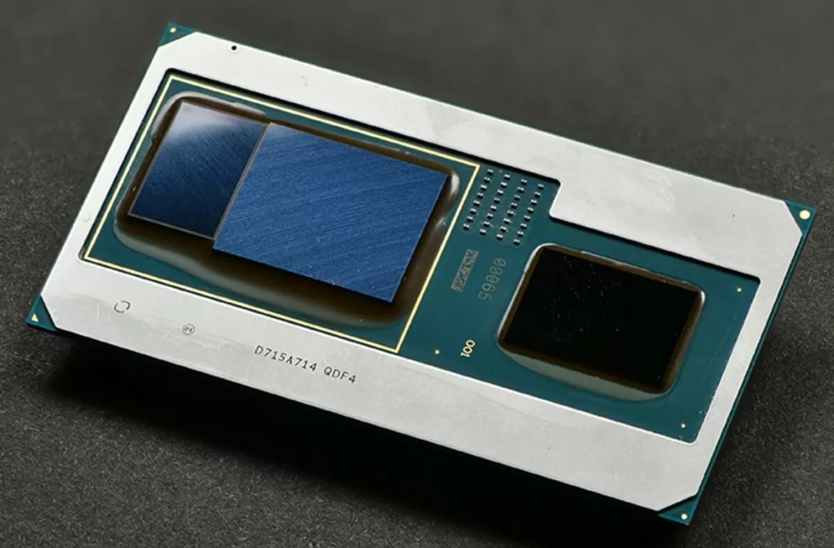
Most large chip companies have recognized the importance of these trends and have been working on advancing their various chiplet-related technologies for the last several years. To that end, Intel just announced some important new additions to its arsenal of chip packaging capabilities at the Semicon West conference this week, all designed to enable even more sophisticated, more flexible, and better yielding chiplet-based products in the years to come. At past events, Intel has talked about its EMIB (Embedded Multi-die Interconnect Bridge) technology, which provides horizontal, or 2D, connections across different chiplet elements. They've also talked about Foveros, which is their 3D stacking technology for putting multiple elements in a chip design on top of each other. The latest development is a logical combination of the two, which they call Co-EMIB, that enables both 2D-horizontal and 3D-vertical connections of components in a single package.
In order to efficiently deliver power and data to these various components, Intel also developed a technology called ODI (Omni-Directional Interconnect), which works through and across chips to provide the power and low latency connections needed to perform closer to monolithic chip designs. Finally, the company also announced a new version of their AIB (Advanced Interface Bus) standard called MDIO that provides the physical layer connect for die-to-die connections used in EMIB.
Together, the new advances give Intel more flexibility and capability to build increasingly sophisticated chiplet-based products---the real fruits of which we should start to see later this year and for several years to come. In addition, these developments help to address some of the challenges that still face chiplets, and they should (hopefully) help to drive more interoperability across multiple vendors. For example, even though the interconnect speeds across chiplets are getting faster, they still don't quite meet the performance that monolithic designs offer, which is why a technology like ODI is important.
In terms of interoperability, there have been some notable examples of chiplet designs that combine pieces from different vendors, notably the Kaby Lake G, which combines an Intel CPU core from Intel's 14nm+ process with an AMD GPU built on Global Foundries 14nm, along with HBM (High Bandwidth Memory). However, right now more vendors are focused on their own inter-chip connection technologies (NVLink for Nvidia, Infinity Fabric for AMD, etc.), although there have also been some industry-wide efforts, such as CCIX, Gen-Z and OpenCapi. Still, the industry is a very long way away from having a true chip-to-chip interconnect standard that would allow companies to use a Lego-like approach to piece together chiplets from whatever processor, accelerator, I/O, or memory elements they would like.
"The industry is a very long way away from having a true chip-to-chip interconnect standard that would allow companies to use a Lego-like approach to piece together chiplets from whatever processor, accelerator, I/O, or memory elements they would like."
Practically speaking, Intel recognizes the need to drive open standards in this regard, and they have made their AIB (and now, MDIO) standards available to others in an effort to help drive this advancement. Whether or not it will have any real-world impact remains to be seen, but it is an important step in the right direction. Particularly in the world of AI-specific accelerators, many companies are working to create their own chip designs that, ideally, could dramatically benefit from being combined with other components from the larger semiconductor players into unique chiplet packages.
At Baidu's Create AI developer conference in China last week, for example, Intel talked about working with Baidu on Intel's own Nervana-based NNP-T neural network training processors. Baidu has also publicly talked about its own AI accelerator chip called Kunlun (first introduced at last year's Create conference), and although nothing was said, a logical connection would be to have future (or more likely, custom) versions of the NNP-T boards that incorporate Kunlun processors in a chiplet-like design.
Though they represent a significant diversion from traditional semiconductor advances, it's become abundantly clear that the future of the semiconductor industry is going to be driven by chiplets. From this week's official launch of AMD's 3rd generation Ryzen CPUs---which are based on chiplet design principles that interconnect multiple CPU cores---to future announcements from Intel, AMD, Nvidia and many others, there's no question that the flexibility that chiplets enable is going to be critically important for advancements in semiconductors and computing overall. In fact, while there's no doubt that improvements in process technologies and chip architectures will continue to be important, it's equally true that advances in the previously arcane worlds of chip packaging and interconnect are going to be essential to the advancement of the semiconductor industry as well.
Bob O'Donnell is the founder and chief analyst of TECHnalysis Research, LLC a technology consulting and market research firm. You can follow him on Twitter @bobodtech. This article was originally published on Tech.pinions.