Bottom line: Intel executives love to tell a good story about the company's ability to innovate and do it fast enough to catch the competition, but it's difficult to take them seriously when the actual products are always on the horizon. Still, the chip giant says it's making important progress on advanced process technologies that will move out of the lab in 2024 at the earliest.
Industry watchers have had their eyes set on Intel's 3nm-based technologies, which are expected to debut in consumer CPUs as soon as next year. In the meantime, the company seems to be hard at work on more advanced process nodes such as Intel 18A and 20A that are central to its future as a semiconductor giant.
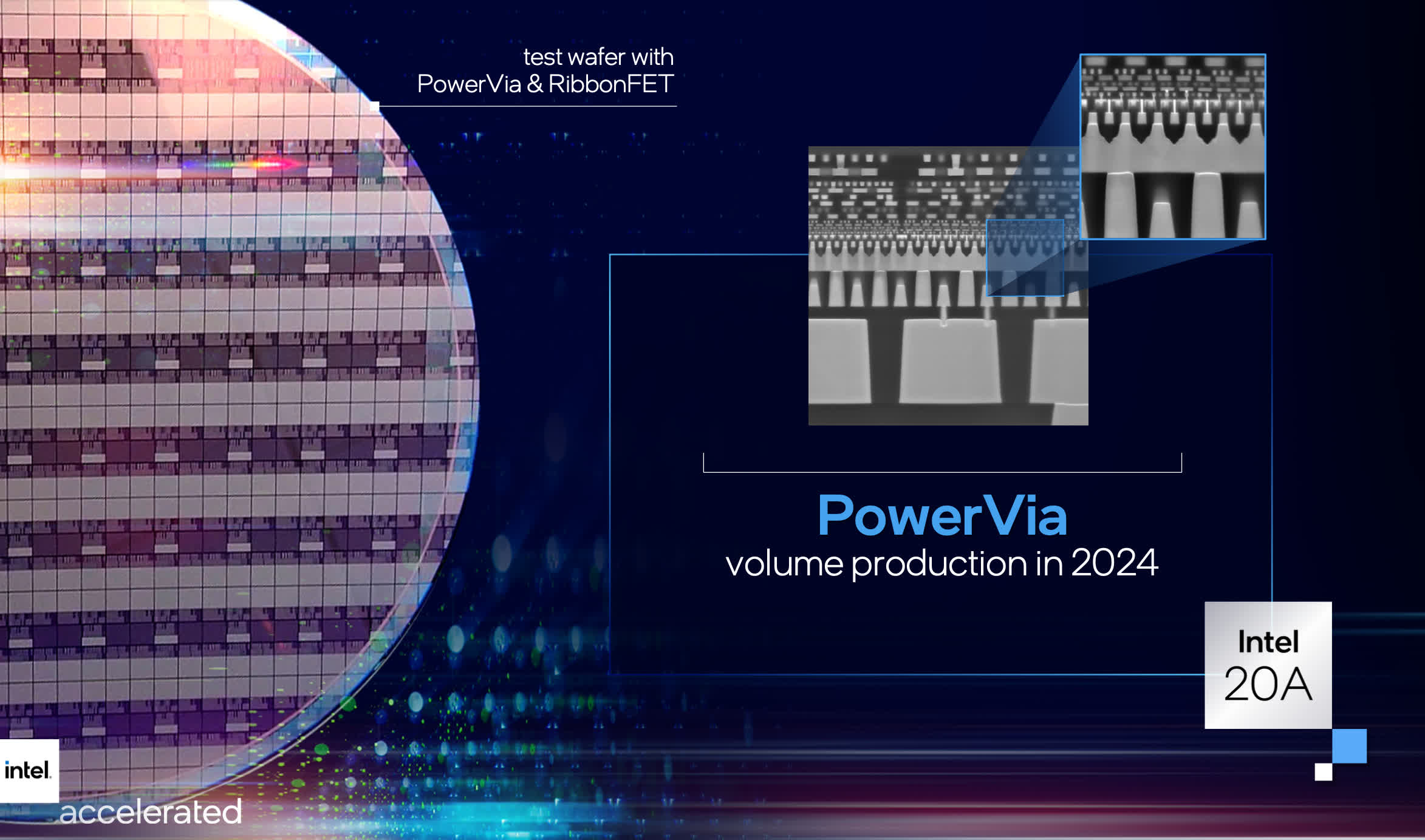
According to a Taiwanese news outlet, Intel's Foundry Services division has finished the tape-out process for the two fabrication technologies. The publication cites the senior vice president and chairman of Intel China, who explained the first chips based on an Intel 18A process could be made in a trial run sometime in the second half of 2024. However, mass production of commercial products based on it isn't planned to start until 2025.

Both Intel 20A and Intel 18A are based around something called gate-all-around FET transistors (GAAFET), which is a common theme for all foundries developing process nodes where the transistor gate pitch is smaller than 3nm. Intel's version of this is called RibbonFET and represents a major design change since the introduction of FinFET in 2011.
Another advantage of Intel's new tech is backside power delivery (called PowerVia). At least in theory, this should allow for higher logic densities, higher boost clock speeds, and lower power leakage --- leading to more energy-efficient designs that are expected to outperform those produced by companies like Samsung Foundry or TSMC.
Also read: How did TSMC get so good?
This is a huge bet that could help Intel's Foundry Services division secure large chipmaking contracts in the coming years while making its products more competitive with Arm-based and AMD designs. It's also a risky and costly transition as it requires adding several steps to the manufacturing process and using additional materials and equipment when compared to previous nodes.

Time, however, is not on Intel's side. The company made efforts to ensure it would be the first to use bleeding-edge ASML Twinscan EXE scanners with 0.55 NA optics for the Intel 18A node, but this would have led to delays it can't afford. As a result, the company has chosen to rely on existing EUV machines to bring the process to market faster.
Whether or not this strategy will pan out as planned is anyone's guess, but suffice it to say analysts aren't nearly as optimistic as Intel CEO Pat Gelsinger. The general sentiment is that the company is in a very bad place, and not just because of lower consumer demand, the rise of homegrown silicon, or the constant cost-cutting going on across the organization. Intel's Foundry Services ambitions are a long-term dream that isn't expected to materialize before the end of this decade.
