Asrock P55 Extreme – Design
If you are coming from a P45 motherboard you will undoubtedly notice the P55 platform gets a more compact cooling treatment.
Although the P55 chipset is still manufactured using a 65nm manufacturing process as was the P45, it's TDP (Thermal Design Power) has been reduced to a mere 4.7 watts. The older P45 chipset pumped out almost 80% more heat with a TDP of around 22 watts.

The new P55 chipset is far less complex as it doesn't have to carry a memory controller, which takes up a vast amount of space within the chip's package. In fact, much of what the north bridge traditionally does has been removed and as a result Intel has integrated the functions of the north and south bridge chipsets into a single chip, which they call a Platform Controller Hub (PCH), in this case otherwise known as the P55.


The heatsink on top of the P55 chip measures 7 x 7cm and is just 1cm tall. The die surface of the P55 measures roughly 1 x 1cm, so the actual bulk of the heatsink is about 3 x 3cm. The larger heatsinks can be found cooling the board's power circuitry 8cm long, 3.5cm wide and 3cm tall. There are two of these heatsinks and each cools 10 MOSFETs, which are part of the board's 8 + 2 power phase.

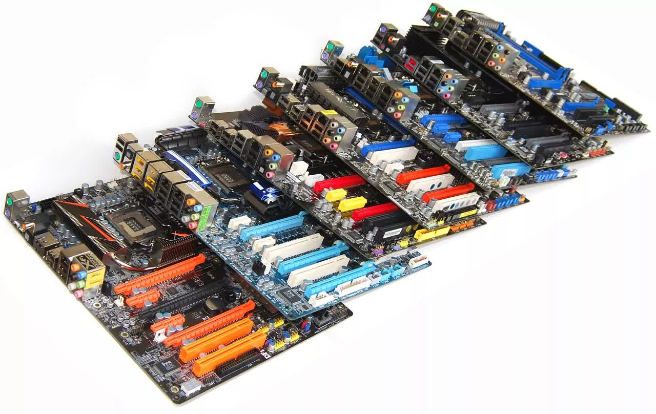
In terms of expansion almost all P55 motherboards will support at least two PCI Express x16 slots, while many will feature three.
The Asrock P55 Extreme does provide you with three PCIe x16 slots, though it is important to note that using two of these with Crossfire or SLI technology will only provide x8 bandwidth each. Additionally, the P55 Extreme features a single PCIe x1 slot and three traditional PCI slots.
The primary and secondary PCIe x16 slots have been separated by a PCI and PCIe x1 slot to help improve air-flow between dual graphics cards, a design that most motherboard manufacturers today use.
The only problem with the Asrock layout is that it features the CMOS battery between the these PCIe x16 slots making it impossible to access with even one graphics card installed.

Another small issue with the board's design is the DIMM slot placement, which is very close to the primary PCIe x16 slot. While it is barely possible to install/remove memory modules with a graphics card installed, it is a bit of a squeeze and the DIMM slot clips will hit the graphics card. Recently Asus solved this issue by simply removing the clips at the bottom of the DIMM slots. A rather obvious yet clever solution.

The rest of the P55 Extreme board design looks very good. The 24-pin power connector is well placed in the top right hand corner of the board where it is accompanied by on-board power and reset buttons. The six SATA ports are mounted at a 90-degree angle to avoid any conflicts with longer graphics cards.

We liked the P55 Extreme's ability to use both LGA775 and LGA1136 coolers. Asrock has made a clever move by including both sets of mounting holes allowing a majority of LGA775 coolers to work with this motherboard. This feature could potentially save users money as they may find their current aftermarket heatsinks to work just as well with their new motherboard.
Looking at the I/O panel we have a pair of legacy PS/2 ports, a CMOS reset button, 7 USB 2.0 ports, eSATA port, Firewire port, LAN port, optical and S/PDIF ports along with six audio jacks. All in all, everything the user could want or need can be found on this I/O panel.

Although the board's appearance is not exactly important, it does seem to play a role for many consumers, which doesn't play too well for the P55 Extreme. While this is certainly not a bad looking motherboard, it tends to look average when sitting next to other boards from ASUS, MSI, DFI or Gigabyte.

Overall we are pleased with the design and layout of the Asrock P55 Extreme as there are no serious design flaws. The board's cooling is sufficient, the layout caters well for multi-GPU setups, while the I/O panel provides all the necessary connectivity.