I've been saying for a number of years that a solid state drive is the single best upgrade you can do to improve your computer's overall performance but the reality is that SSDs haven't been a viable option for mainstream users for a number of reasons. Early drives suffered from lag issues, high prices and low capacities. Lag is now a thing of the past and prices continue to fall but if you need a large amount of high-speed storage, SSDs still aren't the answer.
That could all be changing at some point as a company called Applied Materials has unveiled a new etching system called Centura Avatar that can build vertically-stacked, three-dimensional transistors. This isn't to be confused with 3D manufacturing where 2D chips are stacked but instead refers to actually building 3D NAND structures.
ExtremeTech highlights the price per GB / manufacturing process trend of planar silicon. Dropping from 100nm to 60nm was a huge savings for manufacturers and again going from 60nm to 40nm was beneficial. But after the 20nm milestone, the graph looks pretty bleak and savings aren't really visualized.
The solution is to rethink the manufacturing process by folding a 2D NAND in half and standing it up on its end. Actually accomplishing this task in the real world, however, is very difficult.
According to the folks at Applied Materials, trying to build 3D NAND structures in real life would be like trying to dig a one-kilometer-deep, three-kilometer-long trench with walls exactly three meters apart, through interleaved rock strata --- and that's before we discuss gate trenches or the staircases.
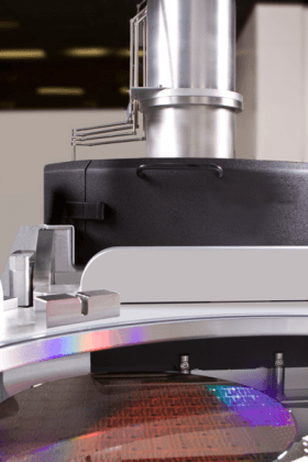
Realistically, it will probably be another few years before we see the Centura Avatar find its way to mainstream SSD manufacturers but at least builders now have a plan to cut cost/GB and boost die density when the time is right. The company plans to showcase the etching machine at SEMICON West 2012, held July 10-12.