Aiming for Atoms: The Art of Making Chips Smaller

Although the likes of Intel and Nvidia have come under fire from noticeably increasing prices of their chips, the article goes a fair way in explaining why a mid range video card or CPU costs a lot more than it did say 10 or 15 years ago.

Inflation is one normal reason, but the cost of the development and manufacturing of ever smaller processes has risen rapidly. Simply going from 28nm to 7nm has doubled the cost of a wafer. On immature processes for a new, tinier, ever more difficult to develop node, the yields will often be less. This also affects relevant memory fabrication, although innovations in that field have helped. Therefore costs are easily more than doubled to tape out a 7nm chip than a 28nm one.

This in the space of just 7 years. Yes, Nvidia and Intel have exploited their technology leads by raising prices. Welcome to the world of capitalism. However a large proportion of those price rises are still down to the underlying steep increase in the costs of developing and manufacturing the parts.

That's why what is often classed today as a mid range video card (RTX2060) is now $350 and not the $200 it (7600GT) generally was in say 2006.
 
Last edited:
Two comments. First, EUV is nominally 13 nm, 193 nm is DUV, these stand for Extreme Ultraviolet, and Deep Ultraviolet respectively. All three dies in the Ryzen R7 3900X are made entirely with ArF 193 nm lithography, but it is very different from the initial ArF litho. Today's litho uses immersion (in water) to get a higher Numerical Aperture, a measure of focusing power. It is not clear whether Intel's 10 nm process uses some EUV exposure steps, it didn't originally. TSMC's current N7 (7 nm) process uses all DUV, their N7+ process, just now starting production, uses EUV for three exposures per wafer.

Also, higher prices for consumers, when they are higher, are not due to the (huge) costs of moving to a new process node. The manufacturers for every semiconductor product do a simple calculation. Will the money saved by moving to the next process node be more than the cost to move? If not, stay at the current process node. This is why skipping the 20 nm node made sense for a lot of manufacturers, even more skipped 10 nm. AMD and GF came up with a low cost to migrate 12 nm node, but even then AMD did not move all of their products from 14 nm. The math didn't justify it.

However, semiconductor manufacturers are not immune to inflation in other areas, So even though prices for the semiconductors themselves have dropped relative to inflation, other costs have not. You can still get a graphics card for $150 that is a huge improvement on the $150 card of 10 years ago. The complication that users face is that in a few years the card they buy today will be unsatisfactory given their increased expectations. Buying a more expensive card less often is a way to reduce costs.
 
Also, higher prices for consumers, when they are higher, are not due to the (huge) costs of moving to a new process node.........Will the money saved by moving to the next process node be more than the cost to move?

This is usually the main consideration when you aren't working with the highest complexity, largest chips.

Manufacturing process matters a lot less if you are building sound chipsets, or network controllers, or I/O processors. Simpler designs. Extreme transistor density for maximum performance is not the primary design goal. Cost considerations outweigh cutting edge performance in most of those cases. Margins are very tight in these sectors. Small chips are built in big volumes per wafer for a couple bucks each. Going to a brand new expensive smaller node gains you effectively nothing significant for a larger manufacturing cost. You lose money in an extremely competitive market, with dozens of other players. You have to wait until the cost per wafer drops so the math works, as you said.

But when you are talking about higher end CPU and GPU design- parts where performance or performance per watt (mobile) is critical, the gains are too irresistible to ignore despite the inevitable much higher cost of taping out a new chip for that node. In general, you have to go to a newer node when they are reasonably mature or you fall behind your competitors.

You especially try and go to that new node as soon as you can make it work if you're a big player with only a handful of direct competitors. Apple, Qualcomm, Samsung, Intel, AMD, Nvidia etc are usually chasing it to deliver the best products they know they can sell at a premium price, higher than the previous generation. Justifying that with significant gains. This drives the industry forward.....

The main reasons why this specific high performance area of the industry wouldn't chase a newer node that hard is when development of the node (or product intended for it) is not shaping up well. Maybe it's not a big gain for the application, or it's delayed, perhaps yields are poor. Sometimes the next, better node is close anyway at that stage and the cycle is short. 20nm TSMC you mentioned was classic case in point, with Nvidia calling it 'worthless' and AMD deciding after evaluation it wasn't well suited to high end chips. Or another (rarer) case might be you don't need to transition quickly because your arch is already way better than the competitor so you're reaping big margins as long as you can (cough, Nvidia Pascal/Turing, Intel Skylake.)

For the big players where that ultimate, market leading performance is king for these companies, you do whatever it takes to reach the next level. You just pass the cost onto an eager consumer hungry for the next perceptible step.
 
Last edited:
"Light isn't actually used -- even for chips like the old Pentium, it's too big. You might be wondering how on Earth light can have any size, but it's in reference to wavelength. Light is something called an electromagnetic wave, a constantly cycling mixture of electric and magnetic fields."

Just outright hilarious, that someone could fail to define the photon so magnificently in 2019. Charge theory is 15 years old now and people still don't know what light is. Incredible. They literally don't believe their own eyes.
 
Yes, I see someone has already noted that 193 nm is not extreme ultraviolet - and since GlobalFoundries gave up on going far below 14nm, and it's processes at 10nm or 7nm that may, optionally, use EUV (Intel's 10nm doesn't, but an experimental 10nm process at IBM did; TSMC's current 7nm, in the Ryzen 3000 chips doesn't, but their new 7nm+ will) what they're using definitely isn't EUV.

Also, making details smaller than the wavelength of light you use involves stuff like double patterning, which the article missed mentioning. And, of course, stuff like double patterning wouldn't even be possible if it weren't for optical proximity correction - sharpening corners on the mask so that rounded corners caused by diffraction are cancelled out.
 
Two comments. First, EUV is nominally 13 nm, 193 nm is DUV, these stand for Extreme Ultraviolet, and Deep Ultraviolet respectively. All three dies in the Ryzen R7 3900X are made entirely with ArF 193 nm lithography, but it is very different from the initial ArF litho. Today's litho uses immersion (in water) to get a higher Numerical Aperture, a measure of focusing power. It is not clear whether Intel's 10 nm process uses some EUV exposure steps, it didn't originally. TSMC's current N7 (7 nm) process uses all DUV, their N7+ process, just now starting production, uses EUV for three exposures per wafer.
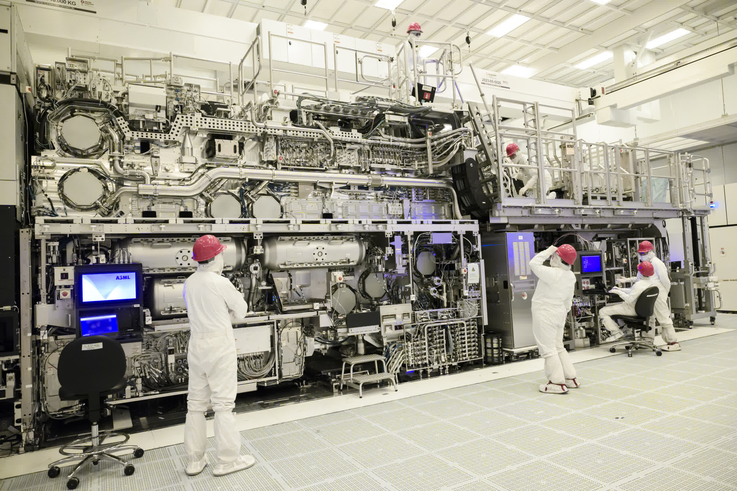
It's these kind of comments and feedback that makes the TechSpot community what it is. I admittedly glossed over important details - one to keep things quite concise and two, it provides the opportunity for a more in-depth follow up by the likes of William Gayde. :) However, errors should be corrected and the identifier acknowledged; if Julio feels that the piece needs an appropriate edit, I'd be happy to include (and credit) your notes.

Also, higher prices for consumers, when they are higher, are not due to the (huge) costs of moving to a new process node. The manufacturers for every semiconductor product do a simple calculation. Will the money saved by moving to the next process node be more than the cost to move? If not, stay at the current process node. This is why skipping the 20 nm node made sense for a lot of manufacturers, even more skipped 10 nm. AMD and GF came up with a low cost to migrate 12 nm node, but even then AMD did not move all of their products from 14 nm. The math didn't justify it.

However, semiconductor manufacturers are not immune to inflation in other areas, So even though prices for the semiconductors themselves have dropped relative to inflation, other costs have not. You can still get a graphics card for $150 that is a huge improvement on the $150 card of 10 years ago. The complication that users face is that in a few years the card they buy today will be unsatisfactory given their increased expectations. Buying a more expensive card less often is a way to reduce costs.
Again, very salient points. All business decisions are driven by costs vs revenue, but the costs of developing fabrication methods, and adapting chip designs for them (or vice versa) have grown, and considerably so. Such costs are only ever going to be passed down to the consumer. Of course, prices for products more often than not simply reflect the market targetted and the expectations therein - this is part of AMD's reasoning behind no longer aiming to be "the cheaper option."
 
Yes, I see someone has already noted that 193 nm is not extreme ultraviolet - and since GlobalFoundries gave up on going far below 14nm, and it's processes at 10nm or 7nm that may, optionally, use EUV (Intel's 10nm doesn't, but an experimental 10nm process at IBM did; TSMC's current 7nm, in the Ryzen 3000 chips doesn't, but their new 7nm+ will) what they're using definitely isn't EUV.
Again, I went for simplicity - perhaps too much so. The UV boundaries are rather blurry; for example, I could have said "Far UltraViolet" which would fit the wavelength range but it's not a term one often reads alongside microchip fabrication.

Also, making details smaller than the wavelength of light you use involves stuff like double patterning, which the article missed mentioning. And, of course, stuff like double patterning wouldn't even be possible if it weren't for optical proximity correction - sharpening corners on the mask so that rounded corners caused by diffraction are cancelled out.
There was lots missed out ;). The actual fab process is worthy of one or two separate articles altogether. I apologise if readers feel that the article doesn't give the topic sufficient justice.
 
One point, though. EUV is basically anything smaller than 193 nm or so. So if a foundry is using 30nm UV instead of 13nm, they can still legitimately claim to be using EUV.

More important to be understood by the layperson is, what is it that makes EUV "extreme"? 193nm is already very short-wave UV - enough to give you a really nasty sunburn.

Basically, most ultraviolet light can be manipulated like visible light, with both mirrors and lenses. But the very short wavelength UV that is EUV can't any more. It has to be treated more like soft X-rays. It won't go through any known material for lenes. And even conventional mirrors won't work either - EUV can be reflected from a mirror, but only at a very shallow angle of incidence.

So instead of parabolic mirrors, to focus EUV, one needs very complicated hyperboloidal shapes. I remember seeing pictures of that kind of mirror in connection with orbiting X-ray telescopes, but the same principle is required for EUV.

Since they're already making chips with 10nm feature sizes without EUV, while 60nm light is officially EUV, there's no point in going to all the trouble and effort of using EUV if you still also have to use double patterning and so on to make your chip. Something on the order of 13nm to 20nm - which still doesn't bring in any (well, not too many; there were some technical challenges every step of the way, I'm sure) new wrinkles after you've cracked the barrier at around 193nm - being a wavelength equal to twice the feature size is what's needed to get the benefits. (Since TSMC's 7nm is a bit of a marketing designation, and is similar in density to Intel's 10nm, 19nm, say, would be good enough.)

EDIT: I've checked, and in fact, the plasma light sources used for current EUV do produce light in the 13.3-13.7nm range.
 
Last edited:
More important to be understood by the layperson is, what is it that makes EUV "extreme"? 193nm is already very short-wave UV - enough to give you a really nasty sunburn.
Indeed! The industry's use of the term EUV is slightly at odds with astrophysics world's use of the term, as the latter defines between the range of 10 and 121 nm, so on that basis, 193 nm isn't EUV - one could use FUV or even UVC. I'm not sure the fab industry would be happy to use FHTSUV ("Flipping heck, that's small UV") but you never know, it might catch on!
 
The UV boundaries are rather blurry; for example, I could have said "Far UltraViolet" which would fit the wavelength range but it's not a term one often reads alongside microchip fabrication.

That is one specific point that is in error, as noted in the post I was making about the same time as yours. The earlier post about this was by someone more technically knowledgeable about this than I am, but he made one mistake which I was correcting in that post.

Yes, what they're using today for EUV lithography is light between 13nm and 14nm in wavelength. But that isn't part of the definition of "extreme ultraviolet". Light with a wavelength of 100nm would still be extreme ultraviolet. Which is why it was never used in making microchips.

Extreme ultraviolet is ultraviolet with such a short wavelength that you can't handle it with normal lenses and mirrors - not even with tricks like immersion lithography to increase the numerical aperture, like they do with 193nm light. It's very much more difficult to work with.

Attempting to use 100nm light would involve the costs of going to EUV - going to fancy hyperboloidal mirrors to focus light, having to work in vacuum - but without much of the benefits, since the process node is so much smaller than that, multiple patterning is still required to only a slightly lessened extent.

Which is why they went with double patterning and then quadruple patterning - using all sorts of tricks to image details several times smaller than the wavelength of the light being used (which some oversimplified physics textbooks will say is impossible). Right down to the 7nm process used by TSMC for the upcoming Ryzen chips. Making details that small with 193nm, though, is starting to get ridiculous.

Fortunately, they finally managed to make EUV lithography practical - and they had to use light that was significantly shorter in wavelength than what they were using for the effort to yield a benefit. Thus, 13.5nm light, and, at least for this process node, no need for double patterning. Given what they managed to do with 193nm light, of course, no doubt EUV plus double patterning will be good for a few more nodes. And, since the details on a chip need to be a few atoms in size to actually work, doubtless Moore's Law will come to an end in its present form before we start hearing about gamma-ray lithography.
 
Next stop, gamma rays focused by microscopic black holes. It might negligibly rise the prices of the newer chips.
 
Although the likes of Intel and Nvidia have come under fire from noticeably increasing prices of their chips, the article goes a fair way in explaining why a mid range video card or CPU costs a lot more than it did say 10 or 15 years ago.

Inflation is one normal reason, but the cost of the development and manufacturing of ever smaller processes has risen rapidly. Simply going from 28nm to 7nm has doubled the cost of a wafer. On immature processes for a new, tinier, ever more difficult to develop node, the yields will often be less. This also affects relevant memory fabrication, although innovations in that field have helped. Therefore costs are easily more than doubled to tape out a 7nm chip than a 28nm one.

This in the space of just 7 years. Yes, Nvidia and Intel have exploited their technology leads by raising prices. Welcome to the world of capitalism. However a large proportion of those price rises are still down to the underlying steep increase in the costs of developing and manufacturing the parts.

That's why what is often classed today as a mid range video card (RTX2060) is now $350 and not the $200 it (7600GT) generally was in say 2006.
Prices were increased because people would still pay a higher price for better performance. With Ryzen 3000 coming soon, Intel is already lowering their prices by ten to fifteen percent, to keep sales up. A small hit in profit margin is seen as worthwhile to keep market and mind-share. If AMD, or Intel, comes up with a lower priced graphics card, comparably efficient to nVidia's cards in both performance and energy use, we can expect nVidia to lower their prices at that time.
 
Next stop, gamma rays focused by microscopic black holes. It might negligibly rise the prices of the newer chips.

You think you jest. Wakefield accelerators are being developed to replace the huge technical and physical investment necessary for something like the LHC. Wakefield accelerators currently work with electrons, but that's all right, that's what you need for an undulator or a wiggler to provide X-rays or gamma rays. Semiconductor labs are currently using synchrotrons in R&D. I don't expect synchrotrons in fabs, but wakefield accelerators are much smaller and easier to operate.

Current EUV steppers or scanners will have a fairly nice fit to 5 nm. The next step is 4 nm or 3 nm (your choice of names, really about 3.5 nm) with double and quad patterning. There are still problems with EUV. (Pellicles, and metrology tools are the biggest remaining.) But the real problem is the transistors. FinFETs allowed the running jump from 28 nm planar to 7 nm. To go much beyond may require a new transistor type, probably gate all around (GAA). The best GAA transistors in the labs though use nanosheets or nanotubes for the source to drain. For chips with billions of transistors these may be grown in place (additive manufacturing instead of subtractive manufacturing).

In any case, getting below about 5 nm will require almost heroic efforts. Not that EUV and FinFETs didn't...
 
The industry's use of the term EUV is slightly at odds with astrophysics world's use of the term, as the latter defines between the range of 10 and 121 nm, so on that basis, 193 nm isn't EUV

Since the semiconductor industry was using 193nm light for ages, and when they said "we're going to start using EUV", they ended up using 13nm - 14nm wavelength light when they did, I'd say the semiconductor industry and astrophysicists are in perfect harmony.

According to Wikipedia, though, EUV ranges from 10nm to 124nm, not 121nm. Not that such a minor correction really matters, but...

A photon of light with a wavelength of 124nm has an energy of 10eV.

A photon of light with a wavelength of 10nm - shorter wavelength, so higher-energy photons - has an energy of 124 eV.

When I saw that, I thought, gee, astrophysicists (if they, and not, say, plasma physicists, are responsible for this) must really like to confuse people. (Unless they just wanted to make it easier to memorize Planck's constant.)
 
Last edited:
You think you jest.

Oh, he was jesting. A Wakefield accelerator is certainly a lot easier to handle than a microscopic black hole.

But after quadruple patterning with EUV, there won't be enough atoms to make working wires and transistors, I would have thought. (7 nm doesn't need double patterning; with it, it should be possible to go to 3 nm - details 1/3 the size of half the wavelength. Quad patterning would go to 1nm, and I thought the atomic limit got hit before that.)

But they're already working with gate-all-around transistors, one thing you mentioned, so maybe they will go below 3nm.

Look at how much smaller 14nm is than 193nm. So if they can make 14nm chips with 193nm light, then with 14nm light, they ought to be able to make 1nm chips with 14nm light. So the Wakefield accelerators would be for even smaller process nodes. If such things could even exist. However, the semiconductor companies wouldn't spend money on looking into Wakefield accelerators without reason, so no doubt my analysis is oversimplified for some reason. Such as - it was such a real pain to make 14nm chips with 193nm light, that switching from EUV to gamma rays would be easier.
 
When I saw that, I thought, gee, astrophysicists (if they, and not, say, plasma physicists, are responsible for this) must really like to confuse people.
Ha! All too true - the fact that there is an ISO standard for solar irradiance values kinda proves this point.
 
@Nick Evanson
Great read. There is but one error. The article states that the atomic diameter of a Silicon atom is 0.1nm. It's actually 0.0111nm(111pm). Thus all of the math used by that measurement needs adjustment.
 
No worries - it's always good to have readers examine and query/question things. I still find it rather mind-boggling that certain parts of modern CPUs really are just a handful of atoms in dimensions.
 
Incidentally, while one Wikipedia page gave my 10 - 124 nm definition of EUV, another one gave your 10 - 121 nm definition of EUV. So it wasn't even a small error on your part, there are slightly different definitions out there.
 
The scientific community as a whole has yet to agree on the boundary between Violet and Ultraviolet so there are variations depending on where you look it up.

Huh? 121nm or 124nm is the boundary between deep ultraviolet and extreme ultraviolet. As for the boundary between violet and ultraviolet, that would be 400nm or 380nm, as violet is a color of visible light.
 
If this doesn't instill in every tech lover a shade of respect for these companies, I don't know what will. These guys are almost fighting atoms and we ***** in forums about how our o/c failed and how X is better than Y.

Not saying criticism is not needed in a healthy market, but sometimes we really overstep our bounds.

Great read!
 
Back