
In the realm of computer chips, bigger numbers are often better: more cores, higher GHz, and greater FLOPs, are all desired by engineers and users alike. However, there's one metric that works in reverse: the smaller, the better. Welcome to the world of semiconductor manufacturing and the technology node, also known as the process node.
But what is it exactly, and why does it keep shrinking? Why is it measured in nanometers, and why are the numbers 5, 3, and 2 now the talk of the industry?
The race for smaller transistors is no longer driven solely by smartphones or computers, but it's being fueled by artificial intelligence. The explosive demand for AI accelerators and massive LLM training hardware has turned advanced chipmaking into both a strategic asset and a bottleneck for global compute capacity. Big Tech companies are pouring tens of billions of dollars into building and buying the chips that make AI possible.
Let's take a journey into the world of process nodes...
The Meaning of Feature Size

But before we dive in, it might help if you've read our CPU architecture series. In part one, we break down how processors work, and in part two we look at how engineers plan and design chips. The most relevant piece for this article comes in part three, where we explain how chips are physically built. If you want deeper context, especially on photolithography, that's where to go – here, we're zooming in on a concept we only touched on briefly:
One of the biggest marketing terms associated with chip fabrication is the feature size.
In the chip industry, feature size is tied to the process node. Historically, it referred to the smallest gap inside a transistor layout. Today, the definition has stretched and blurred – the number printed on the box isn't always the number etched onto silicon. Different manufacturers measure it differently, and process labels like "5 nm" or "3 nm" no longer map cleanly to literal geometry.
In other words, these days, the process node is more of a marketing term and not very useful for comparing production methods. Nonetheless, the transistor remains a critical feature of any processor, as groups of them perform all of the number crunching and data storage done inside the chip.
But even if "nm" has become a marketing shorthand, shrinking nodes within the same manufacturer still signals a real leap in density, efficiency, and performance. And that's why – despite all the fuzziness – smaller remains the holy grail.
Why Smaller Transistors Matter
No activity in the processor world happens instantaneously, and every operation demands electrical energy. Larger components take more time to change states. Signals require more time to traverse, and it takes more energy to circulate electricity within the processor. Put simply, larger components occupy more physical space, making the chips themselves bulkier.

In the above image, we observe three vintage Intel CPUs. From left to right: a 2006 Celeron, a 2004 Pentium M, and an older Pentium from 1995. Their process nodes are 65 nm, 90 nm, and 350 nm, respectively.
To put it another way, the critical parts in the 28-year-old design are over five times larger than those in the 17-year-old model. Another noteworthy distinction: the newer chip houses approximately 290 million transistors, while the original Pentium boasts just over 3 million - nearly a hundred times fewer.
While the reduction in process node contributes to the recent design's smaller physical size and its higher transistor count, it undeniably plays a pivotal role in Intel's advancements.

But here's the real kicker: that Celeron generates approximately 30W of heat, whereas the Pentium emits a mere 12W. This heat emanates primarily from the movement of electricity through the chip's circuits. As electricity flows, energy dissipates due to various processes, with the vast majority being released as heat. While 30 is certainly higher than 12, it's vital to remember that the Celeron boasts nearly 100 times more transistors.
Given that a smaller process node offers the advantages of more compact chips packed with more transistors that can toggle more swiftly – translating to a higher number of calculations per second – and lesser energy released as heat, it naturally raises a question: Why isn't every chip in the world manufactured using the smallest possible process node?
Let There Be Light! (Kind of)

At this point, it's essential to understand a process called photolithography. Here, light passes through a device known as a photomask, which obstructs light in certain areas and allows it to penetrate in others. Where the light passes through, it's intensely concentrated into a small area. This light then interacts with a special layer used in chip manufacturing, delineating the positions of the chip's various components.
Consider it analogous to an X-ray of your hand: the bones block the rays, acting like the photomask, while the flesh allows the rays to pass, resulting in an image that showcases the hand's internal structure.
Interestingly, actual light isn't employed in this process. Even for older chips like the Pentium, light's "size" or wavelength is too large. Now, you might be wondering how on Earth light can have any size, but this is in reference to wavelength. Light is an electromagnetic wave, a perpetually oscillating fusion of electric and magnetic fields.

Image credit: Peellden - Wikimedia
While we often represent it with a classic sine wave to visualize its form, electromagnetic waves don't truly have a distinct shape. Rather, the effects they produce upon interaction adhere to this sine wave pattern. The wavelength of this oscillatory pattern denotes the physical distance between two congruent points on the wave.
Imagine ocean waves lapping at a shore; the wavelength is the distance between consecutive wave crests. Electromagnetic waves exhibit a vast array of possible wavelengths, so we group them under the umbrella term "spectrum."
Small, Smaller, Smallest
In the image below, what we recognize as light is just a minuscule portion of the entire spectrum. This spectrum includes other familiar entities such as radio waves, microwaves, x-rays, and more. Within this spectrum, light has wavelengths approximately around 10-7 meters in size or roughly 0.000004 inches!
For such minute measurements, scientists and engineers favor using nanometers, or "nm" for short. If we delve deeper into a section of the spectrum, we observe that visible light actually spans from 380 nm to 750 nm.

Image credit: Philip Ronan, Gringer
Recall the earlier mention of the old Celeron chip in this article, it was fabricated using a 65 nm process node. You might wonder, how can components smaller than visible light be created? Simple: the photolithography process didn't use light, it used ultraviolet light (a.k.a. UV).
According to the spectrum chart, UV begins at approximately 380 nm (where visible light culminates) and shrinks down to roughly 10 nm. Manufacturers like Intel, TSMC, and GlobalFoundries utilize an electromagnetic wave termed EUV (Extreme Ultraviolet), which has a wavelength of just 13.5 nm. This is the current standard for fabricating chips below 7 nm, and even more advanced version known as High-NA EUV (High Numerical Aperture EUV) is being introduced, allowing the creation of features below 2 nm in size.
These shorter wavelengths not only permit the production of tinier components but also potentially enhance their overall quality. This allows the various parts to be packed in closer together, helping to scale down the overall size of the chip.
Different manufacturers assign distinct names to the scale of the process node they employ. Intel used a catchy name for one of their 10 nm nodes: P1274, but they often represent it as "10 nm" for the lay audience. In contrast, TSMC simply labels theirs as "10FF."
Processor design firms like AMD create the layouts and structures suitable for these smaller process nodes, then rely on manufacturing giants like TSMC for production. TSMC has been diligently advancing with ever-smaller nodes (5 nm, 3 nm), crafting chips for major clients such as Apple, Qualcomm, Nvidia, and AMD. In this realm of manufacturing, some of the tiniest features measure just 6 nm across (though many features are substantially larger).
Most recently, TSMC and Samsung have achieved volume production at the 3 nm level and are preparing for 2 nm nodes, while Intel's "Intel 3" and "Intel 18A" nodes are now shipping. The industry is also shifting from FinFETs to new "Gate-All-Around" (GAA) transistor structures – Intel's version is called RibbonFET – which provide better control over current leakage at atomic scales.
To grasp the sheer minuteness of 2 nm, consider this: the silicon atoms, which constitute the majority of a processor, are spaced about 0.5 nm apart, with each atom being approximately 0.1 nm in diameter. Hence, as a rough estimate, TSMC's 2 nm transistors involve structural elements just a handful of atoms across.
The Challenge in Aiming for Atoms
Setting aside the mind-boggling reality that chip manufacturers are working towards features that span just a few atoms, EUV photolithography has raised a whole bunch of serious engineering and manufacturing challenges.
These challenges have become particularly urgent in the age of AI, where big tech and cloud providers like Microsoft, Google, Amazon, and Meta are deploying tens of thousands of 3 nm-class GPUs and accelerators per data center. Their demand alone has strained global supply chains for high-bandwidth memory (HBM), packaging, and EUV tools.

Intel faced considerable challenges in matching its 10 nm production to the efficiency of its 14 nm process, and GlobalFoundries encountered its own set of problems in scaling down to 7 nm and even smaller. While the complications faced by Intel and GlobalFoundries might not solely stem from the intricacies of EUV photolithography, it's unlikely that the two are entirely unrelated.
The shorter the wavelength of an electromagnetic wave, the more energy it embodies. This higher energy level poses a risk of causing damage during the chip manufacturing process. Ultra-precise fabrication is acutely susceptible to contamination and defects in the utilized materials. Furthermore, factors like diffraction limits and statistical noise – the innate variance in the location where energy from the EUV wave is deposited onto the chip layer – hinder the aspiration of producing flawless chips.

Two manufacturing defects in a chip.
There's also the problem that down in the weird world of atoms, the flow of electricity and the transfer of energy can no longer be assumed to follow classical systems and rules. Keeping electricity, in the form of moving electrons (one of the three particles that make up atoms), flowing down conductors closely spaced together is relatively easy at the scale we're used to – just wrap the conductors with a thick layer of insulation.
However, at the scales where Intel and TSMC operate, this task becomes daunting, primarily because the insulation isn't thick enough. Yet, for now, most production challenges can be attributed to the complexities intrinsic to EUV photolithography. High-NA EUV introduces even greater precision requirements, necessitating entirely new lens systems and resist materials.
Economics and AI Capital
This is because the real problem, the ultimate reason behind the production difficulties, is that Intel, TSMC and all their fabricating chums are businesses, and they're aiming for atoms for the sole purpose of generating future revenue. In a research paper from a few years ago, the following overview was offered as to how much more wafers cost for smaller process nodes...
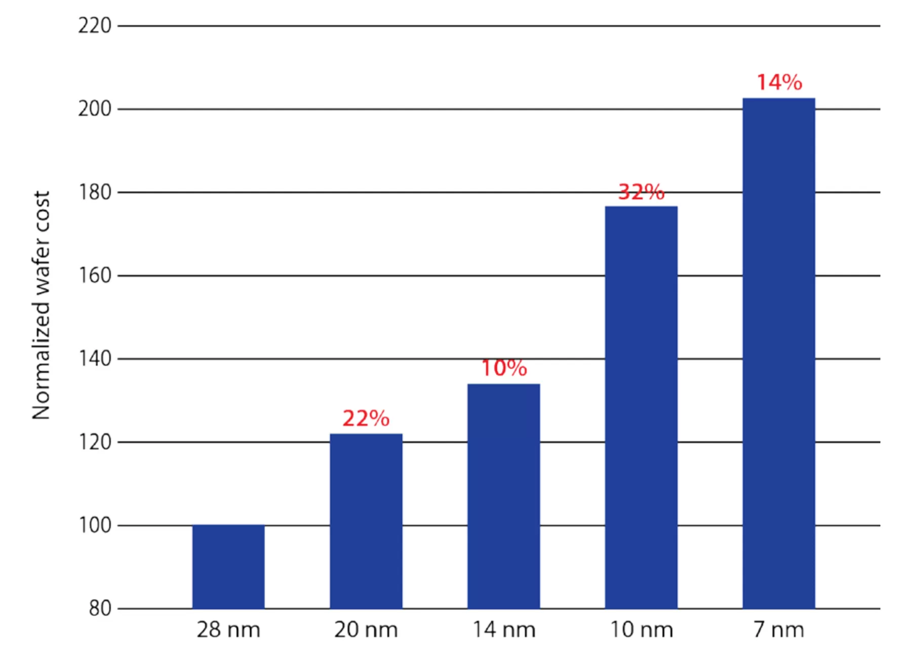
For the sake of argument, let's assume Intel used a 28 nm-class process node for its Haswell CPU series (such as the Core i7-4790K). Under that assumption, transitioning to its 10 nm process would have nearly doubled the cost per wafer. Although wafer yield depends heavily on the size of each chip, smaller nodes can sometimes improve yield by allowing more dies to be cut from a single wafer – partially offsetting the higher manufacturing cost. Even so, manufacturers typically pass at least some of these increased expenses on to consumers through higher prices, while still trying to calibrate those increases against market demand.
During the 2000s and 2010s, the surge in smartphone sales – and the SoCs that powered them – drove the industry to pursue smaller and smaller process nodes. The rapid growth of connected devices in homes and cars added to that pressure, forcing chip manufacturers to absorb financial losses from early, low-yield production runs until their fabrication systems matured enough to produce high-yield wafers reliably.
That economic equation has shifted dramatically in the AI era.
Wafer costs for 3 nm and smaller nodes can exceed $20,000 each, and the cost of designing a new chip can surpass $500 million. To manage these escalating expenses, most high-end processors now adopt chiplet architectures – combining multiple smaller dies on a single package. This approach, popularized by AMD, is now used by Intel, Nvidia, and nearly every major AI accelerator manufacturer to improve yields and flexibility while containing costs.
Much of today's semiconductor investment is now concentrated in AI hardware. Hyperscalers like Microsoft, Google, Meta, and Amazon are collectively pouring more than $250 billion per year into AI-focused data centers. This flood of capital has pulled the entire semiconductor ecosystem into the AI arms race – from foundries and advanced-packaging firms to high-bandwidth-memory (HBM) suppliers and ASML's EUV lithography toolmakers.
Given that the stakes now reach into the tens of billions of dollars for each new fabrication generation, the risks are enormous. This kind of financial gamble was one of the reasons GlobalFoundries withdrew from the leading-edge process race several years ago and now focuses on mature nodes (12 – 65 nm), serving the automotive, industrial, and IoT markets where stability and scale outweigh cutting-edge miniaturization.
Future Prospects
If all of this sounds a little doom-and-gloom, it's worth remembering that the immediate outlook is actually promising. As was predicted years ago, Samsung and TSMC have had 3 nm production lines running for several years, pilot runs for 2 nm are already underway, and Intel is clawing its way back with RibbonFET and PowerVia powering its newest nodes.

Moreover, chip designers are future-proofing their designs by utilizing multiple nodes in their products. AMD's chiplet design strategy with Ryzen CPUs has set a precedent for other chip makers. For example, their 3rd-gen Ryzen CPUs that debuted back in 2019 incorporated two chips made on TSMC's 7 nm node and one 14 nm chip crafted by GlobalFoundries. The former were the actual processor parts, while the latter managed DDR4 memory and PCI Express devices connected to the CPU.
Today, that approach has matured further. AMD's Ryzen 9000 and EPYC Genoa chips use 5 nm and 6 nm chiplets, while Intel's Meteor Lake and Arrow Lake processors employ 7 nm-class tiles integrated through Foveros 3D packaging. This chiplet and 3D stacking revolution has become as important as node size itself.
Meanwhile, AI isn't just the reason fabs are racing forward – it's also becoming part of the toolkit that gets them there. Machine learning is now helping optimize lithography, spot defects earlier, and squeeze a little more yield out of every wafer. The AI boom is both pushing fabrication to its limits and teaching fabs how to survive that pressure.

The chart above shows Intel's process node evolution over the past 50 years. On the vertical axis, the node size is showcased in factors of 10, starting all the way up at 10 000 nm. The chip giant's trajectory suggests a rough node half-life (the time taken to reduce the node size by half each time) of 4.5 years.
That projection proved largely correct: by 2025, Intel, TSMC, and Samsung are all producing chips at the 3 nm class, with 2 nm on the horizon for 2026 – 2027. From here, the gains won't come from shrinking alone, but from going vertical, stacking transistors in 3D, and baking AI acceleration deeper into every layer of silicon.
The result will be chips that are denser, cooler, and dramatically more efficient – the kind that make edge inference in tiny robots feasible, power wearables that barely sip energy, and drive exascale data centers without melting the grid. And surely, graphics hardware (or should we say AI chips?) that surpass the visual marvels of blockbuster films from a decade or so ago.
The future is bright indeed, because the future is small.