Good questions!
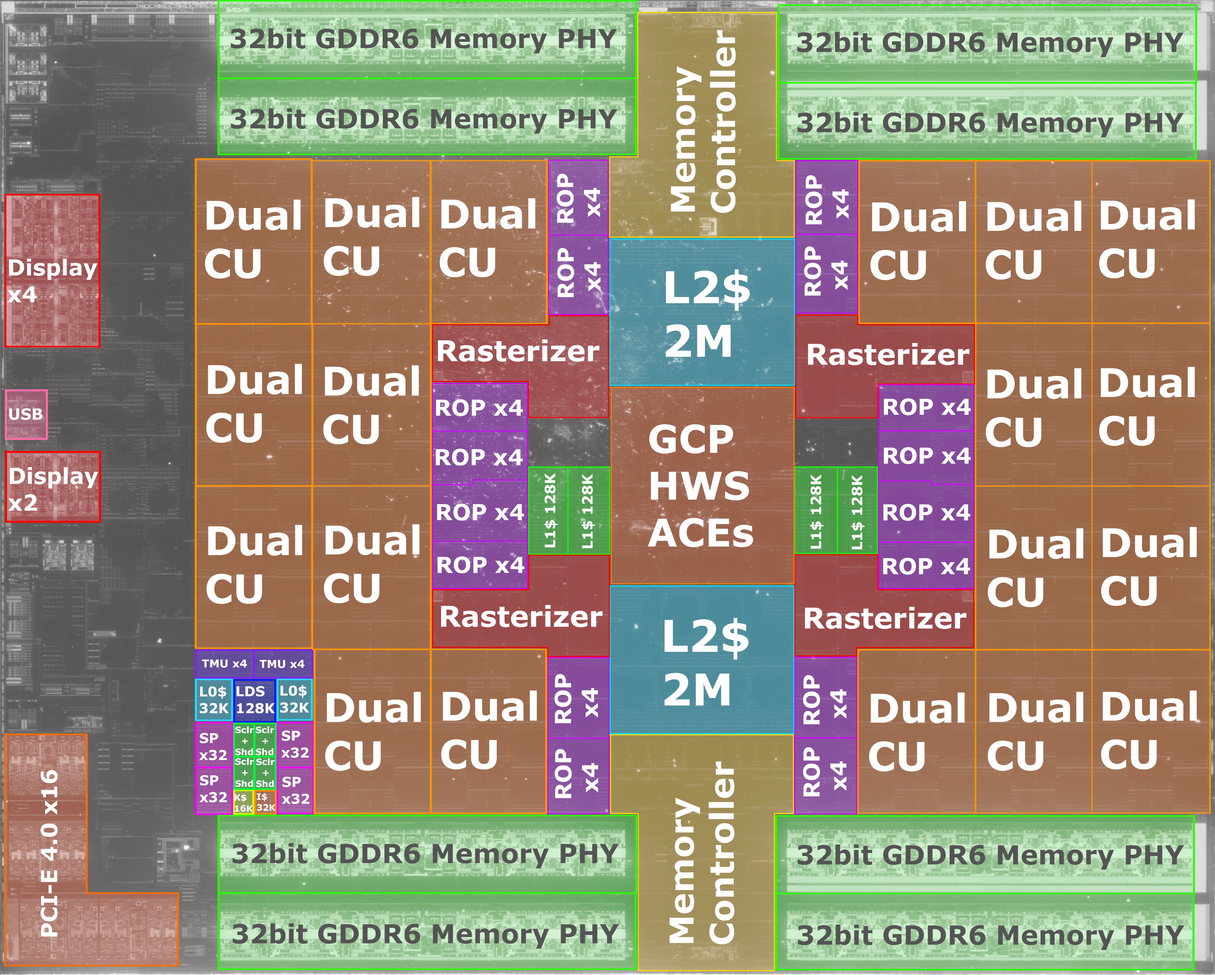
AMD have been working on improving the memory hierarchy of their GPUs for some time now. This has mostly been 'internally' - added an exclusive L0 cache for each CU, enabling CUs within a shader engine to share their L1 caches, giving the L1 caches exclusive access to L2, and so on.
All of this was done in RDNA, with the primary aim of reducing cache misses, which are the bane of any GPU - once you have an L2 cache miss, then the latency really piles in (thanks to off-die DRAM accesses). But slapping in more L2 causes design problems, as it's tied to the memory controllers and takes up a lot of die space.
However, their CPUs have been packing lots of high density L3 cache for a good while, with Zen 2 and 3 having 32 MB of L2 victim cache per CCD. It's a lot more dense than normal GPU cache (something like 4 times more) so while AMD were designing Zen 2, they were also looking at how this could be implemented into other microarchitectures. But with a key priority for the first Navi chips being that must not be hulking monolithics, the cache system in the RX 5000 series was made 'good enough' for the relatively small number of CUs - it could have been made better, of course, but not for the target die size and price tag.
Neither RDNA nor RDNA2 were about being big - just having more DX12 functionality and better efficiency - but AMD were planning for big Navis right from the start. The RDNA2 chips in the consoles are 56 and 36 CU variants (Xbox. PS respectively) so not quite large enough to really benefit from having Infinity Cache, although again that benefit is weighed against die size and product cost (they would have loved to pop in, say, 20 MB of I.C.).
In the case of Nvidia, Ampere currently has two main variants: the GA100 and the GA102/104. The former is absolutely jammed with cache, despite having a 5120-bit HBM2 memory interface: 24 MB of total L1 and 48 MB of L2 cache. The GA102 is lightweight in comparison: 10.5 MB of total L1 and 6 MB of L2 cache. Ampere was designed with both in mind, but with the GA102 already coming in at 628 mm2 (a fair bit smaller than the TU102, but still huge), they couldn't afford anymore die space to add in more L2.
AMD, on the other hand, had the means and know-how to add in another level of cache, without making their chips too big - at 520 mm2, Navi 21 is pretty much twice the size of Navi 10. Not bad considering that it's double in everything else
and has 128 MB of extra cache.
As to whether this means that AMD had planned Infinity Cache right from the very start or it appeared through a case of engineers going 'hmmm, I wonder what happens if we do
this...' will probably get answered when we see RX 6500/6600 models. The RX 5500 XT uses a Navi 14 chip, which is effectively a Navi 10 that's been chopped in half:
The only other Navi 1x variant is the one in the likes of the
Radeon Pro V520 - it seems to be a binned Navi 10, but with a HBM2 memory interface.
So if a smaller Navi 2x is the same again (chopped in half)
and it retains some Infinity Cache, then I would interpret that as being good evidence for it being part of the grand plan from the start. On the other hand, if Navi 21 is the
only GPU that has the cache, then I would see that as being indicative as being a late addition to the design.