ASML pushes EUV power to 1,000 watts, unlocking up to 50% more chips per machine

Skye Jacobs

Posts: 2,006   +58
Staff
The big picture: In a laboratory near San Diego, ASML Holding's engineers have pushed the extreme ultraviolet beams generated inside the company's machines to a new threshold: 1,000 watts of continuous EUV power. The achievement is a technical milestone that could enable chip manufacturers to produce up to 50 percent more semiconductors per machine by the end of the decade, helping ASML maintain its dominant position in one of the most strategically important tech sectors in modern industry.
The achievement, confirmed by ASML technologists Michael Purvis and Teun van Gogh, does not involve a proof-of-concept demonstration or a short-lived experiment. The company says the new light source operates under factory-ready conditions and could be deployed in commercial systems later this decade. It represents a strong response to growing pressure from US startups and Chinese research programs seeking to replicate ASML's complex EUV process from the ground up.

EUV, or extreme ultraviolet lithography, relies on light with a wavelength of just 13.5 nanometers – short enough to etch patterns only a few dozen atoms wide onto silicon wafers. To generate this light, ASML uses a precisely controlled sequence of events: a stream of molten tin droplets, ejected 100,000 times per second, is struck midair by a high-powered carbon dioxide laser. The collision vaporizes the tin into plasma hotter than the surface of the Sun, releasing EUV photons that are then captured by Zeiss-manufactured mirrors and directed onto the wafer.

Doubling the droplet frequency and introducing a second "shaping" laser pulse – rather than relying on a single pulse – proved critical to achieving the 1,000-watt output. The advance is compatible with the company's existing hardware architecture, Purvis told Reuters.
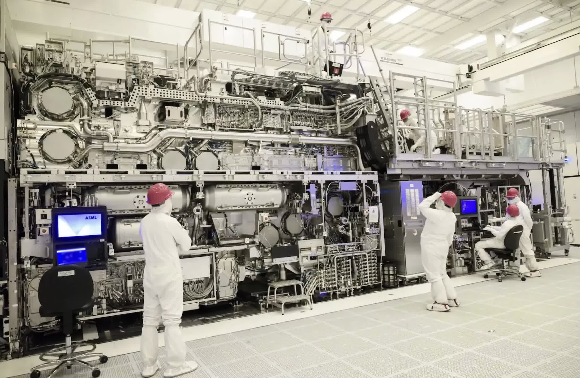
ASML's most recent production models process roughly 220 wafers per hour using 600-watt EUV sources. With the 1,000-watt systems planned for rollout before 2030, throughput could exceed 330 wafers per hour. Each wafer contains hundreds to thousands of semiconductor devices, depending on design complexity.

Shorter exposure times enabled by a more powerful light source also help reduce the overall cost per chip. "We'd like to make sure that our customers can keep on using EUV at a much lower cost," said van Gogh, who oversees ASML's NXE platform.

The development also advances the company's long-term objectives. ASML believes the design principles could eventually scale to 1,500-watt or even 2,000-watt light sources.

Such progress does more than improve chip yield – it also intensifies the global competition to develop alternative EUV manufacturing systems. ASML remains the only company capable of shipping commercially viable EUV lithography machines, a position that has prompted the US and Dutch governments to restrict technology transfers to China. Those controls, in turn, have accelerated Beijing's efforts to develop comparable systems domestically.

Meanwhile, American startups are advancing rapidly. Substrate and xLight have attracted hundreds of millions of dollars in private and government funding to develop what they claim could become next-generation lithography tools. In late 2025, the Trump administration announced up to $150 million in potential investment in xLight, signaling Washington's intent to support the development of a domestic alternative to ASML.

Even as challengers emerge, experts emphasize that the underlying physics remain extremely challenging. "It's very challenging because you need to master many things, many technologies," said Jorge Rocca, a laser physicist at Colorado State University whose laboratory has trained several ASML engineers. "What was achieved – one kilowatt – is pretty amazing."

Permalink to story:

 
By restricting ASML's ability to sell to China, the US is gambling with the company's future. Light lithography isn't the only path forward. Electron beam etching, using technology similar to CRT drivers (without mirrors), can also be viable.

While a single electron beam is too slow for mass production, speed scales linearly with the number of beams. A machine employing lower EUV to print simpler circuit parts and approximately 250,000 electron beams for the finer details could potentially achieve maximum speeds of 20-40 wafers per hour. Thus, ten such (potentially very cheap) machines might match the output of one ASML machine. These machines could also offer better yields (partly due to their potentially more controlled, slower operation) and, using electrons, could etch much finer details at sub-1nm scales.

If denied access to the latest ASML machines, China will eventually develop this alternative approach at scale. This could render traditional light-based lithography obsolete, as electron-beam systems don't suffer from the "diffraction limits" that plague light lithography and they are much cheaper (1/1000 of the price of an ASML machine). Electrons possess a much smaller De Broglie wavelength than EUV light, and their slower operation can contribute to achieving much better yields. China already possesses hundreds of lower EUV machines, if they equip each one with an electron beam system, they could potentially print features below 1 nm with yields exceeding 95% at a rate of 20 wafers per hour.
 
This could render traditional light-based lithography obsolete, as electron-beam systems don't suffer from the "diffraction limits" that plague light lithography and they are much cheaper (1/1000 of the price of an ASML machine).
Electron beam lithography suffers from a worse problem: Poisson noise. Each process node that halves feature size requires doubling the dose and thus halving the throughput. So 3nm manufacturing is 4X slower than 7nm, and 16X slower than 14nm.

Mapper Lithography spent 20 years trying to bring a multi-electron beam lithography machine to market -- they intended just 13,000 beams, rather than the 250,000+ you envision, and they still never made it to market. They went bankrupt in 2019. (ASML, interestingly, purchased their IP assets).

I don't know whether the future will include maskless EBL or not. But if it does and China winds up leading the technology, it will be only because we allowed it to happen ... not because we denied them EUV machines in 2026.
 
Last edited:
Electron beam lithography suffers from a worse problem: Poisson noise. Each process node that halves feature size requires doubling the dose and thus halving the throughput. So 3nm manufacturing is 4X slower than 7nm, and 16X slower than 14nm.

Mapper Lithography spent 20 years trying to bring a multi-electron beam lithography machine to market -- they intended just 13,000 beams, rather than the 250,000+ you envision, and they still never made it to market. They went bankrupt in 2019. (ASML, interestingly, purchased their IP assets).

I don't know whether the future will include maskless EBL or not. But if it does and China winds up leading the technology, it will be only because we allowed it to happen ... not because we denied them EUV machines in 2026.
China is not a startup with a few engineers and limited resources; if something is physically possible, they can achieve it. Consider ASML, for example: they had to overcome numerous problems. The lenses needed cooling to remain stable at the nanometer scale, but they ended up pre-heating them instead. Surface distortions of just a few picometers ruined the circuits. The laser had to hit every fast-moving, tiny droplet with 100% accuracy three times. The base holding the wafer had to move with high acceleration at ultra-high precision. Hydrogen flow was required to prevent carbon buildup on mirrors.

The problem you describe is a simple adjustment to the photoresist material (less sensitive but more stable). With electron beam lithography, they can directly write on boron-based chips (such as boron arsenide or boron nitride for "fences"), which can achieve speeds up to 10 GHz. Boron dissipates heat much better (ten times better) than silicon and reduces the "energy per bit" to near the Landauer Limit, the absolute theoretical minimum energy required to flip a bit.
 
" To generate this light, ASML uses a precisely controlled sequence of events: a stream of molten tin droplets, ejected 100,000 times per second, is struck midair by a high-powered carbon dioxide laser. The collision vaporizes the tin into plasma hotter than the surface of the Sun, releasing EUV photons that are then captured by Zeiss-manufactured mirrors and directed onto the wafer."

Crazy technology. The future is scary :)
 
This will, of course, result in an absolutely HUGE price drop in things like graphics cards, CPU's and all the other wonderful products reliant on TSMC's output.....................Thank you so much ASML.


/s
 
You wonder how long ASML will continue not selling to China. The agreement was made under the previous administration when the US was a normal democratic country and an ally and not the current basket-case with a strange soft spot for Putin. They are a Dutch company and given the relationship between the US and Europe now I can't imagine this agreement continuing without the US paying them an awful lot of money.
 
The problem you describe is a simple adjustment to the photoresist material (less sensitive but more stable).
Shot noise isn't affected by the photoresist; it's a basic consequence of the statistical nature of quantum mechanics. And if solving the problems with volume production with EBL were simple adjustments that would lead to "1000X cheaper" machines, China would already be developing those instead, rather than desperately attempting to purchase ASML's products.
 
" To generate this light, ASML uses a precisely controlled sequence of events: a stream of molten tin droplets, ejected 100,000 times per second, is struck midair by a high-powered carbon dioxide laser. The collision vaporizes the tin into plasma hotter than the surface of the Sun, releasing EUV photons that are then captured by Zeiss-manufactured mirrors and directed onto the wafer."

Crazy technology. The future is scary :)
If you haven’t yet seen the Veritasium video on this tech it’s absolutely worth a watch:
 
Shot noise isn't affected by the photoresist; it's a basic consequence of the statistical nature of quantum mechanics. And if solving the problems with volume production with EBL were simple adjustments that would lead to "1000X cheaper" machines, China would already be developing those instead, rather than desperately attempting to purchase ASML's products.
This is the conclusion after reading few relative papers and ~200 pages of detailed analysis of the physics with an AI around that problem:

To eliminate this stochastic limit(which exists and in photo lithography too), they can use a system which is divided into three synchronized stages: (A) a metamaterial cathode (with nanotips from materials with high magnetic anisotropy) that uses nanoscale grids to enforce Coulomb blockade, forcing electrons into a single‑file “conveyor belt” so each emitted electron can be counted, (B) a plasmonic trigger that replaces a continuous beam with femtosecond‑laser pulses, each pulse ejecting exactly one electron via deterministic emission, with a micro‑mirror DLP array selecting which nano‑road receives a pulse and (C) a quantum resist composed of molecular monolayers that reacts only at a precise energy threshold, preventing secondary‑electron blur and ensuring the chemical change is confined to the exact impact point.

A digital pattern is loaded onto the micro‑mirror array, optical laser triggers that fire the single electrons down the selected nano‑roads, and a precise impact on the quantum resist material (molecular monolayers with non linear threshold which, reduce blur) that creates a noise‑free pattern. Critical engineering challenges, thermal noise that can break Coulomb blockade, backscatter (proximity effect) that can expose the resist unintentionally and data‑throughput bottlenecks. Those must be mitigated by cryogenic cooling of the cathode, ultra‑thin resists with high‑voltage beams and on‑chip localized memory at the cathode head.

An extra step could be a spin filtering so by combining Photonics (The Clock), Spintronics (The Filter), and Quantum Electrostatics (The Road-Waveguide) the flow would be: 1 Ordered in Time (Laser Trigger) -> 2 Ordered in Quantity (Coulomb Blockade) -> 3 Ordered in Space (Nano-Road Waveguide) -> 4 Ordered in Physics (Spin-Filtering) -> Coherent Quantum Wave (Output)
 
Last edited:
Back