
Why it matters: Canon has shipped the first example of its nanoimprint lithography equipment to an American research consortium, marking a significant milestone in the commercialization of this innovative chip-making technology. The machine can produce chips without relying on costly and power-hungry DUV or EUV lithography processes, and could be a game changer for chipmakers.
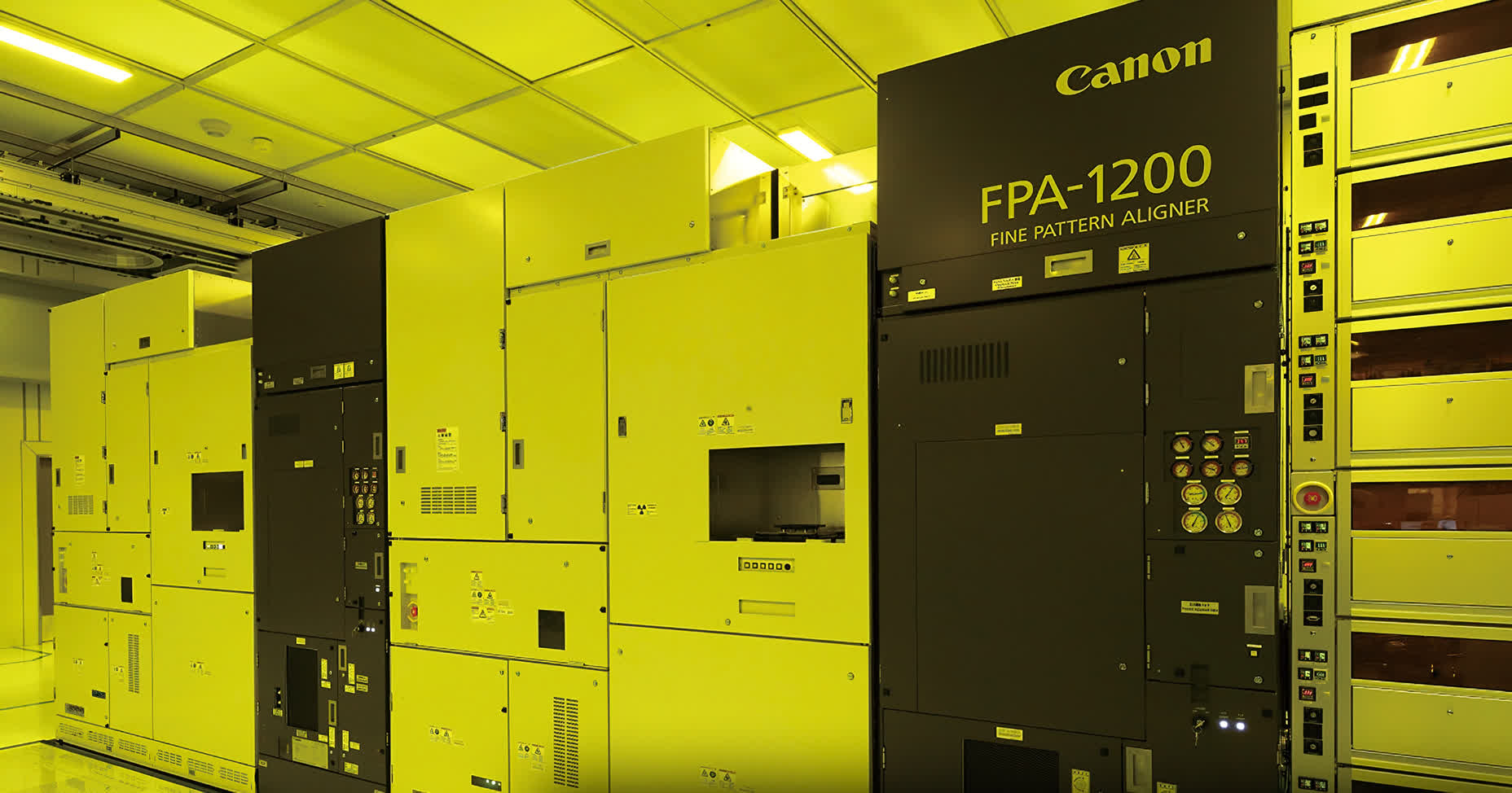
The Texas Institute for Electronics (TIE), a consortium backed by the University of Texas at Austin and comprising semiconductor heavyweights like Intel, recently took delivery of the machinery. Multiple government agencies and academic institutions are also involved.
Traditional semiconductor manufacturing relies on a process called photolithography, in which circuit patterns are projected onto a resin-coated wafer using intense light. Canon's nanoimprint lithography system takes a different approach. Instead of light projection, it physically stamps circuit patterns onto the resin using a mold, a technique that promises significant advantages.
One of these advantages is the potential to reduce manufacturing costs and energy consumption. While conventional photolithography equipment requires arrays of lenses or mirrors, Canon's nanoimprint machines have a simpler design that consumes only about a tenth of the power typically required.
Nanoimprint lithography is also excellent at forming intricate three-dimensional circuit patterns with a single stamp – a feat that would be challenging, if not impossible, with photolithography. This capability could prove extremely useful as chipmakers strive to pack ever-smaller and more complex circuits into their products.
Despite all the potential, some hurdles remain before nanoimprint lithography can be adopted on a broader scale. As highlighted by Tom's Hardware, one challenge is the need for more advanced technology to prevent defects caused by fine dust particles. Partnerships with other companies will also be necessary to develop manufacturing materials compatible with the technique.
Shipping one machine to a research group may seem minor, but Canon's delivery hints at bigger changes brewing in chipmaking. The company's deputy chief executive for optical products, Kazunori Iwamoto, said they aim to sell between 10 and 20 units annually within the next three to five years.
Additionally, by collaborating with Canon's nanoimprint technology, the TIE consortium demonstrates an openness among industry players like Intel, NXP, and Samsung to potentially adopt nanoimprint for future chip manufacturing, which could shake up the industry.
Canon ships first nanoimprint lithography machinery to US consortium backed by leading chipmakers


