Something to look forward to: Intel's 14A node marks a departure from the company's traditional internal design approach. Unlike the 18A process used in this year's Core Ultra 300 "Panther Lake" CPUs, the 14A node was defined through active collaboration with external customers from its earliest stages.
Intel is accelerating development of its upcoming 14A process node, revealing new technical details and strategic updates at the 2025 RBC Capital Markets Global Technology, Internet, Media, and Telecommunications Conference. The company's progress comes amid a high-stakes race to deliver next-generation chips, strengthen its partnership with Nvidia, and maintain ground against rivals pushing the limits of semiconductor fabrication.
Speaking at the industry event, John Pitzer, Intel's vice president of corporate planning & investor relations, said this shift is enabling the company to receive technical and commercial feedback much earlier. That input is helping Intel mature its process development kits to established industry standards. As a result, the company expects meaningful improvements in both performance and yield compared to previous generations.
Two major technological breakthroughs underpin the 14A node's potential. First, Intel is implementing a second-generation Gate-All-Around transistor architecture. GAA differs from legacy FinFET designs by surrounding the channel with the gate, delivering improved control, scalability, and energy efficiency.
Second, Intel is refining its backside power delivery architecture, an engineering approach that separates power-carrying layers from signal paths. This separation enables higher-speed operation and improved thermal management compared to conventional front-side power layouts.
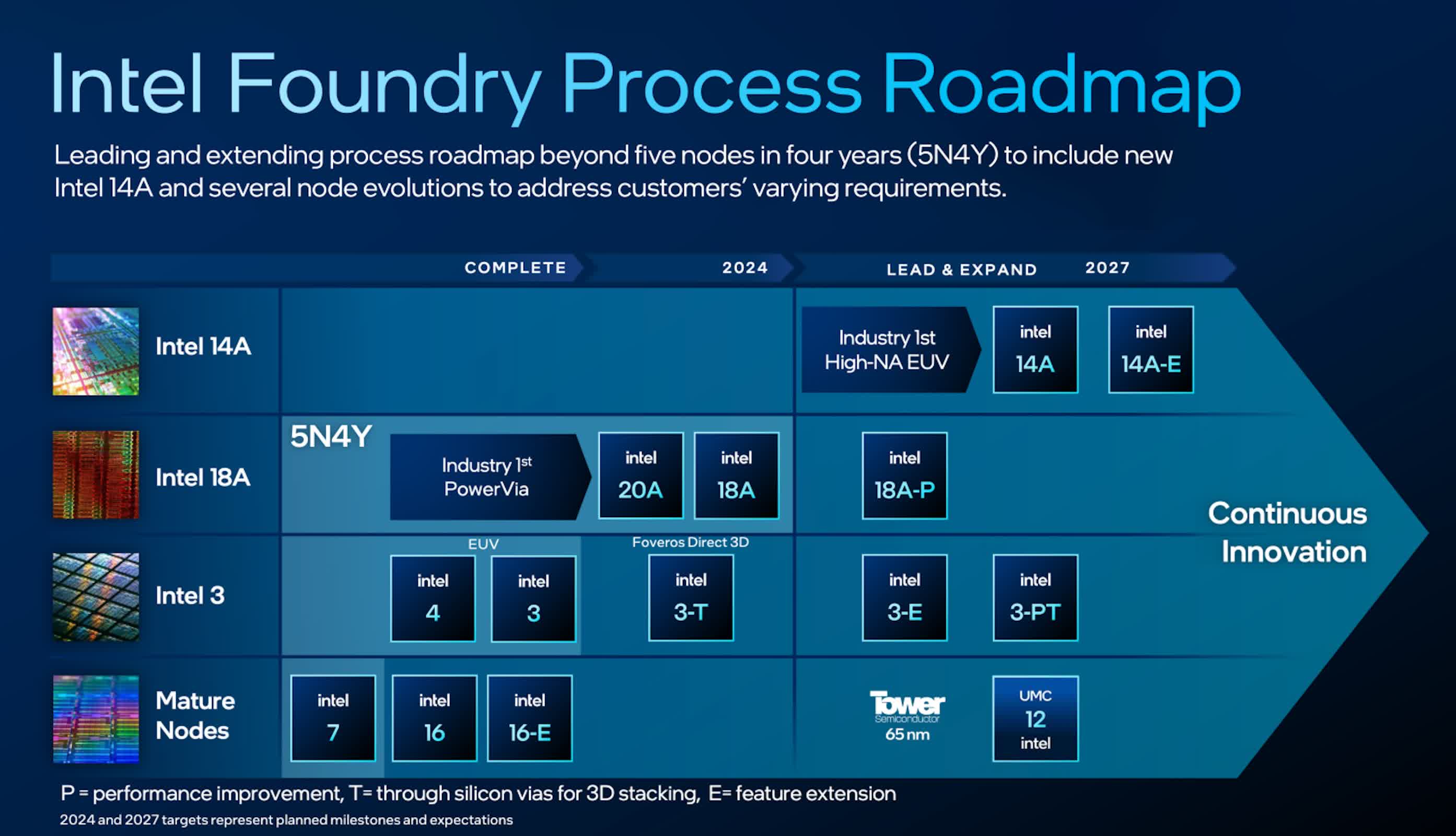
In contrast to the disruptive introduction of GAA and backside power on 18A – which caused notable growing pains – Pitzer said the 14A node benefits from more mature iterations of these technologies and deeper collaboration across the semiconductor ecosystem. He added that engineering teams are "significantly further ahead" in development than they were with the previous node at comparable points in the timeline.
A key element of Intel's evolving strategy is its deepening partnership with Nvidia. According to Pitzer, Intel is set to manufacture a custom Xeon CPU for Nvidia that incorporates NVLink Fusion interconnect technology.
This system allows Intel's x86 processors to access high-bandwidth NVLink networks, enabling the rapid data exchange required for modern AI and HPC workloads. The collaboration also extends to platforms built on Arm's Neoverse architecture, which will be integrated with NVLink Fusion following recent announcements at SC25.
On the consumer side, the $5 billion partnership means Intel will supply the core SoC to original equipment manufacturers, while Nvidia will retain exclusive rights to sell the RTX GPU tile. This arrangement allows for multiple partner configurations and may pave the way for a new wave of high-performance notebooks. While the initial products will target premium segments, both companies indicate the architecture could eventually reach mainstream price points.
Intel deepens commitment to 14A node, develops custom Xeon CPU for Nvidia
