Intel's 18A process hit by low yields and quality issues, putting manufacturing comeback in doubt

Cal Jeffrey

Posts: 4,595   +1,682
Staff member
Editor's take: Intel's long-running manufacturing struggles have cost it money and a CEO, highlighting deeper challenges in reclaiming leadership in advanced chip production. As it relies on TSMC for key parts and wrestles with tight yield targets, the future of its foundry business - and US semiconductor competitiveness - hangs in the balance.

Reuters reports that Intel is facing manufacturing setbacks with its next-generation Panther Lake PC silicon. Only a small percentage of chips produced on the 18A process meet quality standards. Insiders briefed on internal test data say yield was roughly 10 percent this summer – barely an improvement over the five percent figure reported late last year. Intel disputes those numbers but declined to provide its actuals.

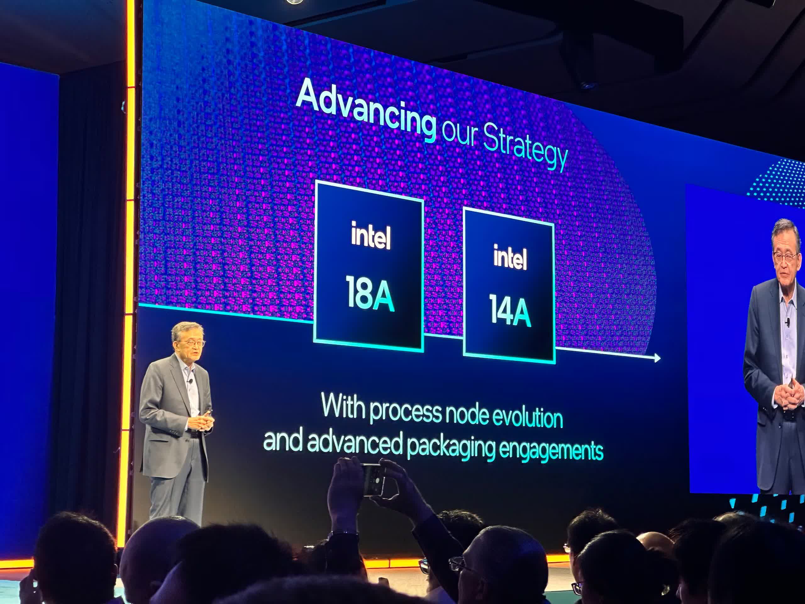
The 18A process introduces a next-generation transistor design and a new method of delivering power to the chip. Intel aims to close the performance gap with TSMC, but some insiders say the company took on too much risk at once. One of the sources likened the effort to a "Hail Mary."

Yields can be hard to track because companies measure them differently. Generally, yield starts low and improves over time. Intel Chief Financial Officer David Zinsner confirmed last month that yields are improving and the company expects to reach production-grade levels by year-end.

"Our expectation is every month they'll get better and better, such that we're at a yield level that is good for production-level Panther Lake at the end of the year," Zinsner told Reuters. "I wouldn't say that margins are accretive even at those yield levels, so we still have to make improvement."

Panther Lake is scheduled for high-volume production in the fourth quarter, slipping behind Intel's earlier forecast for a mid-year launch. Historically, the company waits until yields reach at least 50 percent before ramping output, with profitability typically starting closer to the 70 to 80 percent range. Without a significant improvement, Intel will have to sell chips at reduced margins - or potentially at a loss.

Intel previewed several Panther Lake laptops at Computex in May and maintains the launch is on track. However, sources tinsist that the number of manufacturing defects per chip area remains roughly three times higher than what would be acceptable for mass production.

The company has poured billions into new facilities to support 18A and warned it may abandon leading-edge manufacturing altogether if it cannot attract outside customers – primarily Apple and Nvidia – to its 14A successor. Meanwhile, Intel remains reliant on TSMC to produce parts of its in-house chip designs, including the upcoming Nova Lake, underscoring the challenges it faces in restoring complete manufacturing independence.

Permalink to story:

 
How come Intel can't get contract from nvidia, amd, qualcomm to manufacture their low and midrange products???

They hate to use expensive tsmc for those product ranges anyway and causing their low availability in the consumer market.

Density spec of Intel 3 is similar to tsmc n4.
If Intel manufacture geforce 5060 and 5070 chips, there will be more such cards in retailers
Because their node sucks, production sucks, power use sucks, yields suck.

IF their node was comparable to TSMC n4, then intel would be using it instead of paying for TSMC nodes.
 
The poor yield situation is clearly there given the fact that
1. Broadcom first reported poor yield on 20A,
2. Intel cancelled multiple nodes recently,
3. Intel did not even use their own foundry for current gen CPU and GPU.

If the yield on previous nodes were reportedly poor, changing the node number does not solve the problem. So while Intel sounded very bullish on their 18A, their action speaks the opposite. In fact, when the current CEO said that they will can advanced nodes if they don’t get more external customers to use their foundry, it kind of tells me that he is not confident. If the product is as good as Intel claimed, big tech will flock to them since TSMC is now able to charge them whatever they want as a monopoly.
 
TSMC is achieving 90 % yields, while Intel is only at 10 % ? That looks like a fundamental issue in their workflow, or perhaps they're missing something crucial.

I.e., Using plasma or radiation for environmental purification from VOCs, microbes, and surface contaminants, contact free magnetic levitation to mitigate vibrations, magnetic bearings on critical stages (lithography steppers, wafer spin coatters, etchers).
Eddy current damping for the floor and equipment frames, a conductive (e.g., copper or aluminum) plate is moved relative to a fixed magnet (or vice‑versa). The motion induces eddy currents that generate a resistive magnetic field opposing the motion.
Active magnetic feedback, sensors (accelerometers) feed a controller that adjusts the currents in the bearing electromagnets in real time.

Implementation Details from AI
1 Magnetic Bearing Platform
Base – A flat, rigid plate of high‑conductivity aluminum (≈ 3 mm thick) or a composite with embedded copper layers.
Magnet Array – Arrays of rare‑earth permanent magnets (NdFeB) or, for tunability, arrays of surface‑mounted electromagnets.
Field‑shaping yokes – Soft‑iron yokes to guide the field and create a stable levitation gap.
Control – For electromagnets, a low‑noise current driver with a PID loop that keeps the levitation gap within ±0.1 mm.
Isolation – The bearing sits on a conventional mechanical isolation mount (air‑spring or elastomer) so that the magnetic system only handles the residual vibration.

Benefits
No moving parts → virtually zero wear.
Contactless → no particle generation (critical for clean‑room).
Can be tuned to the resonant frequency of the stage by adjusting the magnetic stiffness.

2 Eddy‑Current Damping Panels
Construction – Copper or aluminum panels (≈ 2 mm thick) bonded to the floor or to the underside of equipment frames.
Magnet Placement – Arrays of NdFeB magnets positioned behind the panels, oriented so that the magnetic flux is perpendicular to the direction of expected motion.
Gap – A small, adjustable air gap (≈ 0.5–1 mm) between magnet and panel.
Effect – As the panel moves, eddy currents flow in the metal, generating a magnetic field that opposes the motion.
Tuning – By changing the magnet strength or the panel thickness, the damping coefficient can be adjusted.

Benefits
Passive, low‑maintenance.
Works over a wide frequency band (10–200 Hz).
No moving parts → no contamination.

3 Active Magnetic Feedback
Sensors – MEMS accelerometers mounted on the stage or on the floor.
Controller – DSP or FPGA running a real‑time algorithm that adjusts the bearing currents to cancel detected vibrations.
Actuators – The same electromagnets used for levitation.
Safety – Fail‑safe mode that reverts to passive damping if power is lost.

Benefits
Can suppress low‑frequency resonances that passive systems struggle with.
Adaptable to changing loads or process steps.
 
Last edited:
TSMC is achieving 90 % yields, while Intel is only at 10 % ? That looks like a fundamental issue in their workflow, or perhaps they're missing something crucial.

I.e., Using plasma or radiation for environmental purification from VOCs, microbes, and surface contaminants, contact free magnetic levitation to mitigate vibrations, magnetic bearings on critical stages (lithography steppers, wafer spin coatters, etchers).
Eddy current damping for the floor and equipment frames, a conductive (e.g., copper or aluminum) plate is moved relative to a fixed magnet (or vice‑versa). The motion induces eddy currents that generate a resistive magnetic field opposing the motion.
Active magnetic feedback, sensors (accelerometers) feed a controller that adjusts the currents in the bearing electromagnets in real time.

Implementation Details from AI
1 Magnetic Bearing Platform
Base – A flat, rigid plate of high‑conductivity aluminum (≈ 3 mm thick) or a composite with embedded copper layers.
Magnet Array – Arrays of rare‑earth permanent magnets (NdFeB) or, for tunability, arrays of surface‑mounted electromagnets.
Field‑shaping yokes – Soft‑iron yokes to guide the field and create a stable levitation gap.
Control – For electromagnets, a low‑noise current driver with a PID loop that keeps the levitation gap within ±0.1 mm.
Isolation – The bearing sits on a conventional mechanical isolation mount (air‑spring or elastomer) so that the magnetic system only handles the residual vibration.

Benefits
No moving parts → virtually zero wear.
Contactless → no particle generation (critical for clean‑room).
Can be tuned to the resonant frequency of the stage by adjusting the magnetic stiffness.

2 Eddy‑Current Damping Panels
Construction – Copper or aluminum panels (≈ 2 mm thick) bonded to the floor or to the underside of equipment frames.
Magnet Placement – Arrays of NdFeB magnets positioned behind the panels, oriented so that the magnetic flux is perpendicular to the direction of expected motion.
Gap – A small, adjustable air gap (≈ 0.5–1 mm) between magnet and panel.
Effect – As the panel moves, eddy currents flow in the metal, generating a magnetic field that opposes the motion.
Tuning – By changing the magnet strength or the panel thickness, the damping coefficient can be adjusted.

Benefits
Passive, low‑maintenance.
Works over a wide frequency band (10–200 Hz).
No moving parts → no contamination.

3 Active Magnetic Feedback
Sensors – MEMS accelerometers mounted on the stage or on the floor.
Controller – DSP or FPGA running a real‑time algorithm that adjusts the bearing currents to cancel detected vibrations.
Actuators – The same electromagnets used for levitation.
Safety – Fail‑safe mode that reverts to passive damping if power is lost.

Benefits
Can suppress low‑frequency resonances that passive systems struggle with.
Adaptable to changing loads or process steps.

If you read some of what's been said about how Intel operated, they were more like small enclaves or fiefdoms. One of the signatures of these people were that once they started down an path, regardless of how is was progressing, they stuck to it no matter what. As a result, they never regrouped or lowered their targets. It was perfection or bust, no matter how long it takes. 10nm was a step too dense to work right (remember Intel stated it was "equal" to TSMC 7nm). Rather than make any changes to the larger goals, the just kept beating the dead horse. That's how we got 14+++++++++++ nm. Seems Pat didn't have enough time to break them of that habit.

Current node doesn't work? Well, we don't have time to fix it, just move on to the next node! We'll get that one right.
 
Back