Massive leak reveals AMD's 'Strix Point' APUs with 16 CPU cores and 3 GHz+ iGPU

DragonSlayer101

Posts: 366   +2
Staff
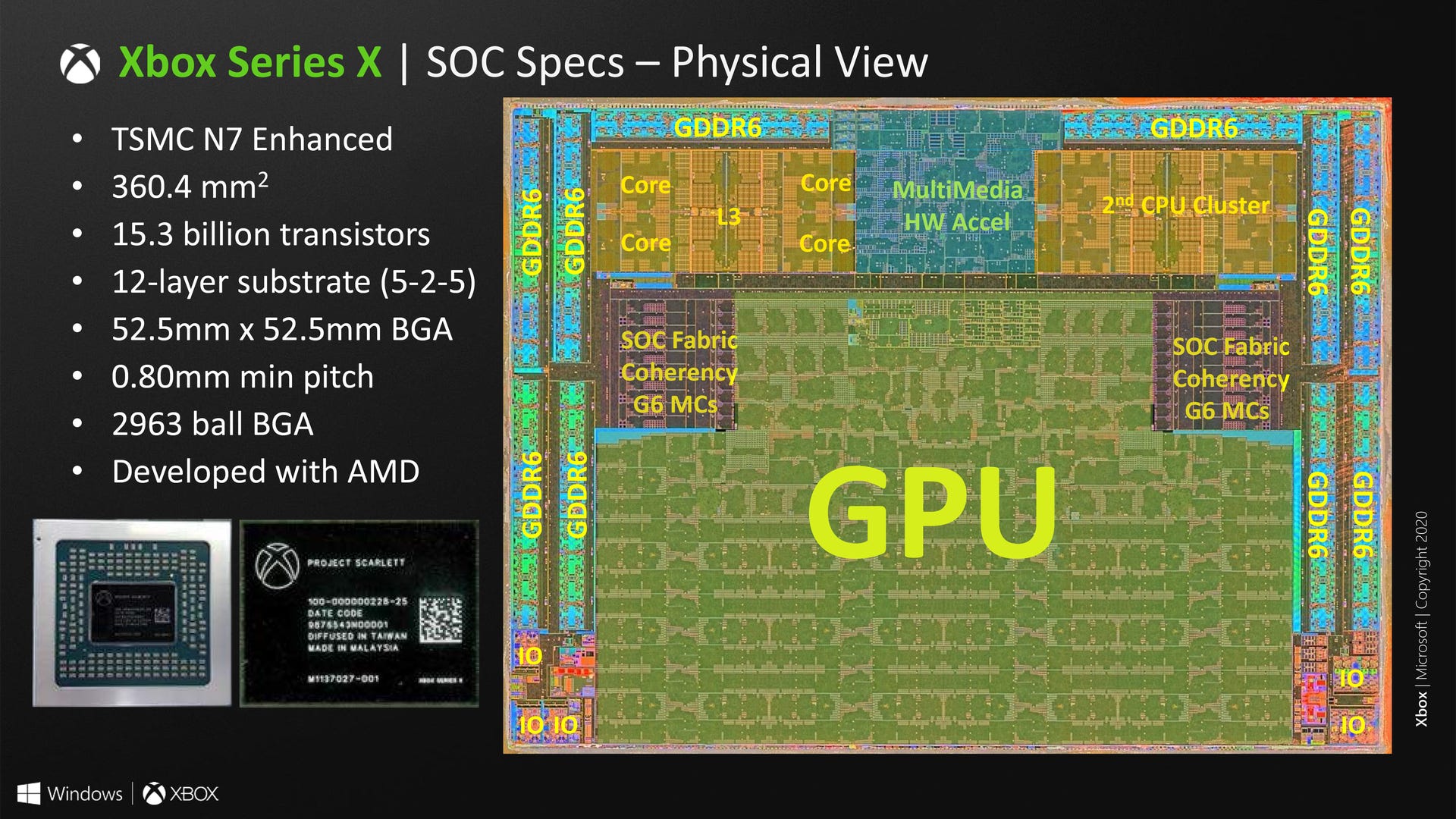
In context: At CES 2023, AMD announced its Phoenix-HS APUs featuring Zen 4 CPUs and RDNA 3 iGPUs. The company is expected to follow that with the 'Strix Point' APUs, sporting Zen 5 CPUs and RDNA 3+ iGPUs. According to AMD's official roadmap, the Strix Point chips will launch sometime in 2024, although the exact ETA remains a mystery for now.

Almost a year after AMD officially teased its 'Strix Point' APUs, popular YouTube channel RedGamingTech has shared many interesting details about the upcoming hardware. According to the video, the flagship Strix Point APU will come with 16 cores, including 8 big Zen 5 and 8 smaller Zen 4D cores, alongside 32MB of L3 cache.

On the graphics side, the chip is expected to feature an RDNA 3+ iGPU with 8 Work Group Processors (WGP). The video also suggests that the iGPU on the most powerful Strix Point APU would have clock speeds of more than 3GHz.

If the reported specs hold up, it would be a little disappointing, as an earlier video from the channel claimed that Strix Point's RDNA 3+ iGPU could have 12 WGP/24 Compute Units (CU) with around 9 TFLOPS of FP32 precision performance.

The channel had earlier claimed that the raw compute power of the Strix Point iGPUs could make lower-end discrete graphics cards obsolete, but it remains to be seen whether that will happen.

Meanwhile, the mid-range Strix Point SKU will reportedly have 4x Zen 5 and 8x Zen 4D cores, paired with 16MB of L3 cache and 4 RDNA 3+ WGPs. Finally, the entry-level chip is said to come with up to 6 cores, including 2x Zen 5 and 4x Zen 4D. They are also tipped to have 8 MB of L3 cache and a 2 WGP iGPU.

The core count, cache and WGPs will not be the only differences between the high-end and entry-level Strix Point APUs. As per the video, the top-end chip in the lineup will be fabricated using TSMC's 3 nm process, while the other two SKUs will use the 4 nm process. The chips are also expected to have a powerful memory controller with support for DDR5-6400 or LPDDR5X-8533 RAM.

The Strix Point APUs will release in 2024, meaning we're unlikely to get an official confirmation about the rumored specs anytime soon. However, expect more leaks from other sources as we get closer to the launch.

Permalink to story.

 
This will likely also be used in mid-gen refreshes of consoles, rumours are starting about PS5 Pro which will finally deliver on some bold performance promises made in the run up to the PS5 launch. I haven't heard any rumours about the Series X/S, but I'm sure they'd be likely to bring one out if Sony does, but they still need to sort out that god-awful naming convention.
 
This will likely also be used in mid-gen refreshes of consoles, rumours are starting about PS5 Pro which will finally deliver on some bold performance promises made in the run up to the PS5 launch. I haven't heard any rumours about the Series X/S, but I'm sure they'd be likely to bring one out if Sony does, but they still need to sort out that god-awful naming convention.
Unlikely if you consider that the PS5 is capable of just over 10TFlops and the XSX is capable of 12+ TFlops. The purported specs here have around 6.2 TFlops max. The GPU/CPU configuration would certainly allow for some efficiencies, but no where near enough to make up that gap, let alone be more powerful than the current consoles.
 
Unlikely if you consider that the PS5 is capable of just over 10TFlops and the XSX is capable of 12+ TFlops. The purported specs here have around 6.2 TFlops max. The GPU/CPU configuration would certainly allow for some efficiencies, but no where near enough to make up that gap, let alone be more powerful than the current consoles.
Ah yeah my bad, I was more thinking about Zen 5 rather than the APUs (though I did think the consoles were using some beefy buffed up APUs)
 
I think it is possible for iGPUs that are as powerful as mid and even high end GPUs, but to get there the total size of the chip would have to be increased. I think this is very doable, but would require a new socket like thread rippers do to accommodate all of those cores. Now that AMD has been pretty successful with MCMs, perhaps this can be done in a way that wouldn't cost an arm and a leg to buy. You would simply have a CPU chiplet and a GPU chiplet and then perhaps even add v-cache. Imagine Navi 31 being placed beside a 7800X3D chiplet, with the same memory chiplets for the Navi. The motherboards would be expensive having to handle 300+ watts to the APU socket and you'd have to get some massive coolers for that thing, but Ryzen is so power efficient. In laptops of course, they couldn't get quite that creative, but perhaps 7800 level GPUs and 125-175 watts of total power. Of course this would all share the same RAM pool, so you would want to get the fastest DDR 5 available, but it would be pretty convenient to have 32 GB+ of RAM. You wouldn't have to worry about running out. I would imagine though you would want to do 4 channel rather than just 2 channel RAM though to increase the bandwidth for the GPU.

The question is, would gamers buy it? Would AMD be willing to try another dedicated APU platform after the A-series flop?
 
Last edited:
I think it is possible for iGPUs that are as powerful as mid and even high end GPUs, but to get there the total size of the chip would have to be increased. I think this is very doable, but would require a new socket like thread rippers do to accommodate all of those cores. Now that AMD has been pretty successful with MCMs, perhaps this can be done in a way that wouldn't cost an arm and a leg to buy. You would simply have a CPU chiplet and a GPU chiplet and then perhaps even add v-cache. Imagine Navi 31 being placed beside a 7800X3D chiplet, with the same memory chiplets for the Navi. The motherboards would be expensive having to handle 300+ watts to the APU socket and you'd have to get some massive coolers for that thing, but Ryzen is so power efficient. In laptops of course, they couldn't get quite that creative, but perhaps 7800 level GPUs and 125-175 watts of total power. Of course this would all share the same RAM pool, so you would want to get the fastest DDR 5 available, but it would be pretty convenient to have 32 GB+ of RAM. You wouldn't have to worry about running out. I would imagine though you would want to do 4 channel rather than just 2 channel RAM though to increase the bandwidth for the GPU.

The question is, would gamers buy it? Would AMD be willing to try another dedicated APU platform after the A-series flop?
Every single time I read something like this, I have to ask myself "why do people just not understand hardware?".

ANY and EVERY tech improvement for said iGPU would also apply yo the dGPUs, which have their own (far faster) memory bus, their own TDP, and their own (far larger) cooling system, and they will, of course, be proportionately faster then any APU could dream of. This has always been, and always be, the case.

Physics doesnt change because you call something an APU.
I never said this would be better than a dGPU. I said "I think it is possible for iGPUs that are as powerful as mid and even high end GPUs" and I said "The question is, would gamers buy it?" The point being that just because it could be done, doesn't necessarily mean its worth doing. There simply has to be a market for it and I doubt there really is at the moment. That being said, for there to be a market for it, someone would have to prove that it could actually be done in such a way that it brings value to the table, at this point, that has not been demonstrated with an APU and its unlikely AMD or anyone else is willing to give it a try right now. I concede that DDR5 would not be equivalent to GDDR6X GDDR7, but, you would at least be able to add enough RAM that you would not have to worry about running out, though, the GPU would likely be bottlenecked by the bandwidth, but that also means you would probably dial it back a little from its discrete counterparts. Still, a Navi 31 GPU in the configuration that I am suggesting, even with DDR5, could still be a pretty stout high-end GPU.
 
Last edited:
I think it is possible for iGPUs that are as powerful as mid and even high end GPUs, but to get there the total size of the chip would have to be increased. I think this is very doable, but would require a new socket like thread rippers do to accommodate all of those cores. Now that AMD has been pretty successful with MCMs, perhaps this can be done in a way that wouldn't cost an arm and a leg to buy. You would simply have a CPU chiplet and a GPU chiplet and then perhaps even add v-cache. Imagine Navi 31 being placed beside a 7800X3D chiplet, with the same memory chiplets for the Navi. The motherboards would be expensive having to handle 300+ watts to the APU socket and you'd have to get some massive coolers for that thing, but Ryzen is so power efficient. In laptops of course, they couldn't get quite that creative, but perhaps 7800 level GPUs and 125-175 watts of total power. Of course this would all share the same RAM pool, so you would want to get the fastest DDR 5 available, but it would be pretty convenient to have 32 GB+ of RAM. You wouldn't have to worry about running out. I would imagine though you would want to do 4 channel rather than just 2 channel RAM though to increase the bandwidth for the GPU.

The question is, would gamers buy it? Would AMD be willing to try another dedicated APU platform after the A-series flop?
Lots of things against such an idea. To have shared RAM between the Zen chiplet and RDNA GCD would require a complete redesign of the IO die, and to provide sufficient bandwidth for the GPU, it would also need to be large and expensive. If one went with a traditional RAM structure (I.e. had removable DIMMs), you'd never get enough bandwidth for the GPU anyway, even with 4 channels, and the latency would be awful. One only has to look at the APU in the PS5, for example, to see how RAM needs to be, if one wishes to how a shared memory system -- non-removable DRAM modules, all soldered onto the board, close to the APU (just as it is on a graphics card).

Then there's the cost. Zen 3/4 CPUs are relatively low in price, because they comprise two to three chips, and none of them are particularly big. The CCDs are just 70 mm2 and the IO die is 125 mm2. The GCD in Navi 31 is 150 mm2, but without the L3 cache, it would take a notable dip in performance, so that would need to be added to the new IO die, increasing its size and cost (it'd have to be a lot bigger anyway).

A new socket, motherboard, and cooling system would all need to be designed, the cost of which would all need to be recouped in the final product. So who would buy such a product? Given that it would be worse than a CPU+dGPU and be more expensive, few people would be willing to do so.
Okay, well, I stand corrected. While I think the rest is technically doable, the RAM issue is bigger than I assumed in my head. I thought with the speed of DDR5 that it might be plausible, but I did not realize the bandwidth differences were as big as they are. Sounds like the only way a decent APU would ever be made would require the RAM to be soldered to the board which would defeat any upgradability, it would basically be a console.
 
Lots of things against such an idea. To have shared RAM between the Zen chiplet and RDNA GCD would require a complete redesign of the IO die, and to provide sufficient bandwidth for the GPU, it would also need to be large and expensive. If one went with a traditional RAM structure (I.e. had removable DIMMs), you'd never get enough bandwidth for the GPU anyway, even with 4 channels, and the latency would be awful. One only has to look at the APU in the PS5, for example, to see how RAM needs to be, if one wishes to how a shared memory system -- non-removable DRAM modules, all soldered onto the board, close to the APU (just as it is on a graphics card).

Then there's the cost. Zen 3/4 CPUs are relatively low in price, because they comprise two to three chips, and none of them are particularly big. The CCDs are just 70 mm2 and the IO die is 125 mm2. The GCD in Navi 31 is 150 mm2, but without the L3 cache, it would take a notable dip in performance, so that would need to be added to the new IO die, increasing its size and cost (it'd have to be a lot bigger anyway).

A new socket, motherboard, and cooling system would all need to be designed, the cost of which would all need to be recouped in the final product. So who would buy such a product? Given that it would be worse than a CPU+dGPU and be more expensive, few people would be willing to do so.
As a theoretical argument, back in the day, some peripherals used to have DMA controllers onboard which allowed them to access DRAM directly (bus arbitration and all that). It sounds like we have moved away from that model with current hardware/motherboard design. I get trace lengths would be longer and would add a minute amount of lag between a GPU and the main memory, and that IO/motherboard design would have to be re-done, but in theory, would it not be possible to move back to such a model? Or would there be other technical issues which would make using a DMA controller unsound?
 
I don’t need 16 cores in a laptop. That’s what my desktop is for.

Give me an 8 core CPU and a beefier GPU (in an ultralight body of course) instead.
You might not need them, but I don't want to have 2 machines. Give me a laptop that can do 95% of what my desktop can do and I'm in. Portability is important to me. I travel between homes frequently and don't want to have a desktop in each home. One, high-end, laptop should do the trick. And, I don't care about battery life as I am never running solely on batteries.
 
I get trace lengths would be longer and would add a minute amount of lag between a GPU and the main memory, and that IO/motherboard design would have to be re-done, but in theory, would it not be possible to move back to such a model? Or would there be other technical issues which would make using a DMA controller unsound?
In APUs used in consoles, DMA is absolutely required because you don't want the CPU cores to be tied up handling DRAM access requests from the GPU. In the case of the Xbox Series X, the DMA controllers are integrated into the SoC Fabric Coherency Memory Controllers:

die_shot.png


Although its not explicitly indicated, the same is also true of the IO die in Zen 4 CPUs -- this chip handles data requests from the individual chiplets and the integrated GPU, again all with DMA:

Zen-4-I-O-Die.2.png


The DMA controller will be buried in the logic circuitry somewhere.

As for the general PC, DMA controllers are usually integrated into the primary devices if they're using PCI Express, like graphics cards do. This is because they're the only device on that bus, so it makes sense for them to negotiate data transactions themselves. However, since the PCIe controller is integrated into the CPU itself (or at least it is for GPU slots), then transaction still gets 'handled' by the CPU -- just not processed directly.
 
I wonder if AMD is going to get sued by Asus for using "Strix"?
I don't know about the sued part but re-using this name struck me as odd too. It's a word I've only ever heard in conjunction with the Asus brand. Why would they muddy the waters like that? Are they considering "AMD Series X" and "AMD Switch" for their next product lines?
 
I don't know about the sued part but re-using this name struck me as odd too. It's a word I've only ever heard in conjunction with the Asus brand. Why would they muddy the waters like that? Are they considering "AMD Series X" and "AMD Switch" for their next product lines?
I wouldn't have done it, however, apparently the word Strix is a type of wood owl so there might not be a case here.
 
Lots of things against such an idea. To have shared RAM between the Zen chiplet and RDNA GCD would require a complete redesign of the IO die, and to provide sufficient bandwidth for the GPU, it would also need to be large and expensive. If one went with a traditional RAM structure (I.e. had removable DIMMs), you'd never get enough bandwidth for the GPU anyway, even with 4 channels, and the latency would be awful. One only has to look at the APU in the PS5, for example, to see how RAM needs to be, if one wishes to how a shared memory system -- non-removable DRAM modules, all soldered onto the board, close to the APU (just as it is on a graphics card).

Then there's the cost. Zen 3/4 CPUs are relatively low in price, because they comprise two to three chips, and none of them are particularly big. The CCDs are just 70 mm2 and the IO die is 125 mm2. The GCD in Navi 31 is 150 mm2, but without the L3 cache, it would take a notable dip in performance, so that would need to be added to the new IO die, increasing its size and cost (it'd have to be a lot bigger anyway).

A new socket, motherboard, and cooling system would all need to be designed, the cost of which would all need to be recouped in the final product. So who would buy such a product? Given that it would be worse than a CPU+dGPU and be more expensive, few people would be willing to do so.

You have to be more clear, that you are speaking about MOBILE APUs...!

Because AMD has a AM5 APU coming out within the next 7-8 months, that will eliminate the need for a 1080P dGPU. (ie: GTX1080ti ~ RTX3050)


This will likely also be used in mid-gen refreshes of consoles, rumours are starting about PS5 Pro which will finally deliver on some bold performance promises made in the run up to the PS5 launch. I haven't heard any rumours about the Series X/S, but I'm sure they'd be likely to bring one out if Sony does, but they still need to sort out that god-awful naming convention.
When consoles get 16 cores PC will finally get over this multiple generation of 8 core stagnation. $450 8 core cpu anyone? Until then yes please.
 
No, I wasn't. EdmondRC was discussing the concept of having something like the Navi 31 GPU paired with a 7800X3D-like CPU in the same package, to which I responded with my comments.

For mobile...?
Because Edmond and InsaneGamer discussion seems like they are talking about MOBILE.


Because we already know the low-wattage Phoenix APU's from AMD with the R7 780M iGPU already takes out low hanging fruit like the GTX1650ti and close to the RTX2050. What AMD's really been holding back on... is what You and Edmond are talking about... is a HIGHER-WATTAGE Phoenix APU (ie: HX), or one with more than 12 CU's..?

Please understand, AMD was not allowed to compete with SONY or Microsoft using their Infinity Fabric, for their own use, for 30 months, per a non-compete clause when inking the PlayStation5/XSX deals. (This is insider info)

That is why you see AMD holding off... before proliferating the industry with tons of APUs.


ps: There is also "technical talk" about how/perhaps AMD's new iGPUs could "talk with" AMD's dGPUs... using SAM/BAR type DMA logic on AMD's up and coming AM5 APUs. So it might be true on mobile applications too?
 
Last edited:
Back