Forward-looking: The engine of the digital age is running up against the laws of physics. Modern semiconductors, the microscopic foundations of computing, are nearing their physical limits just as artificial intelligence and high-performance data processing reach new heights of demand. The result is an industry-wide reckoning... and a search for what comes after the microchip.
Nowhere is this transformation more visible than at Nvidia, whose valuation recently soared to about $5 trillion, making it the world's most valuable publicly traded company. Nvidia's flagship processors are intricate marvels. Each unit – encapsulated in a plastic package and interwoven with copper connections – contains up to 208 billion transistors.
With a single chip priced around $30,000, these components offer unprecedented computational muscle, especially when arrayed by the thousands in data centers. Nvidia's recent architectural breakthroughs enable chips to operate collectively as large-scale hyperscale computers rather than as independent processing units.
AI's exponential compute needs, however, have led to a juncture dictated by the immutable laws of physics. At the heart of chip fabrication is extreme ultraviolet lithography, a process dominated by Dutch equipment maker ASML and its $380 million high-numerical-aperture "Extreme Machine."
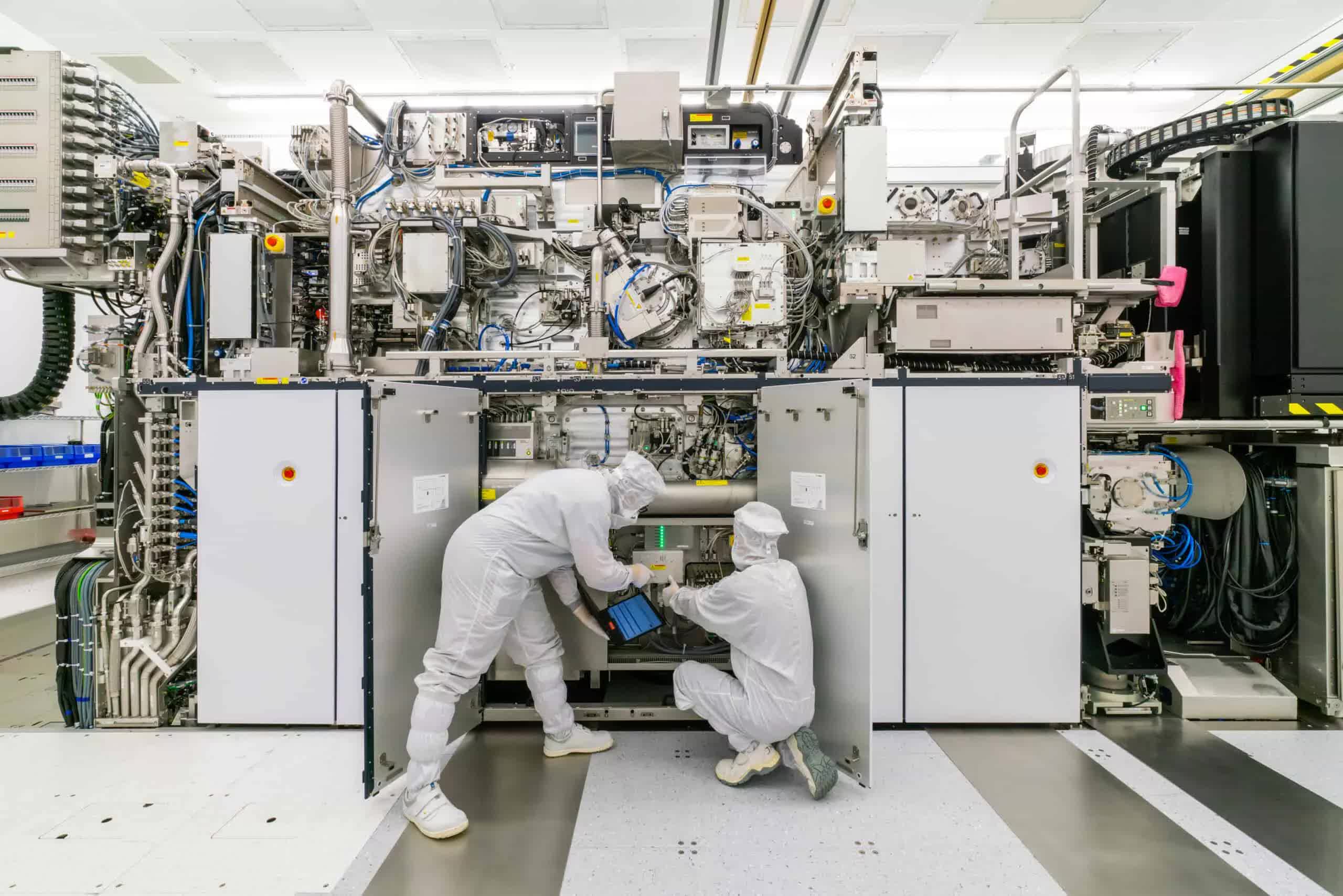
This tool, which resembles a highly specialized camera, flashes light through precision photo masks onto silicon wafers to define circuit patterns.
Despite its sophistication, even the most advanced lithography system faces a fundamental constraint: the reticle limit. This physical law limits the size of a single chip die to about 800 square millimeters. As a result, achieving larger processing capacity requires partitioning computer tasks across multiple smaller chips interconnected by ever-denser packaging, cabling, and fiber links.
These architectural limitations are evident in the evolving design of modern data centers, where the trend is toward smaller "chiplets" interconnected to scale. Yet this fragmentation adds communication overhead, mandates ever more clever packaging innovations, and increases system complexity.
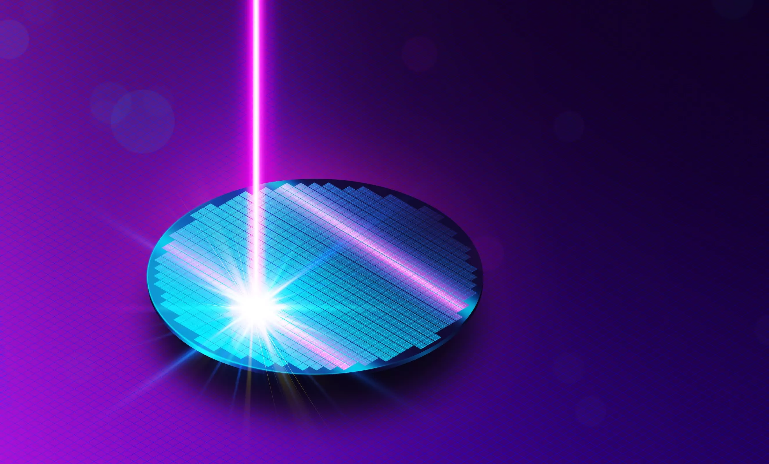
Confronted by both the reticle limit and the diminishing returns of incremental scaling, researchers and semiconductor firms are exploring wafer-scale integration. This model abandons conventional discrete chips entirely, instead using the full silicon wafer as a single, monolithic processing substrate.
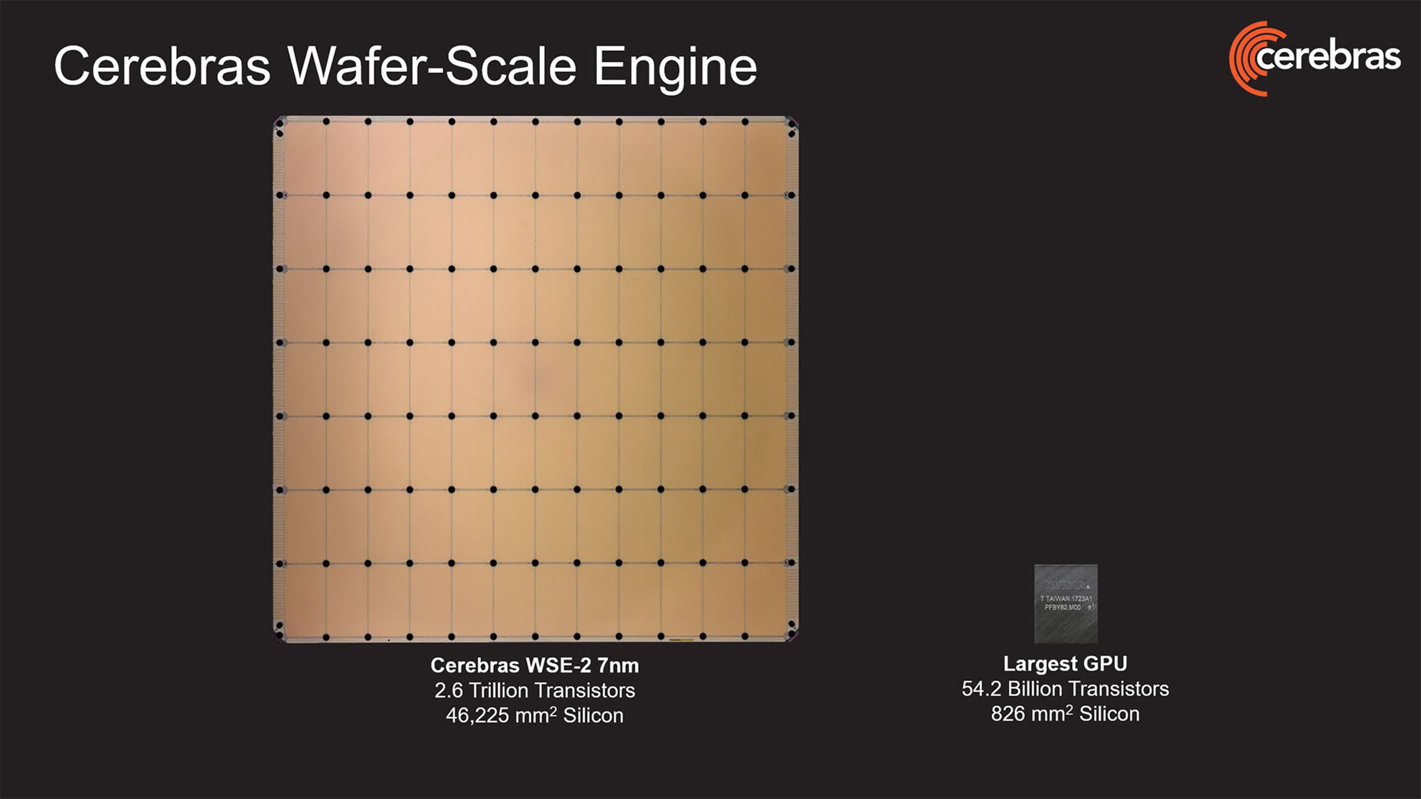
Recent efforts by Cerebras, a Palo Alto company, have yielded the WSE-3 (Wafer-Scale Engine 3), which incorporates four trillion transistors and delivers 7,000 times the memory bandwidth of top conventional chips. Unlike standard architectures, WSE-3 embeds memory directly within the wafer, dramatically reducing latency and shrinking the size of entire data centers.
Tesla, under Elon Musk, experimented with similar concepts in its Dojo project. Though discontinued internally, the approach lives on in ventures like DensityAI.
Lam Research, a major supplier of fabrication equipment, has advanced multi-column electron-beam lithography – through its spinout, Multibeam Corp. – offering manufacturers a pathway to inscribe far larger wafers, bypassing the reticle barrier.
These developments suggest the microchip's reign may soon cede ground to architectures that are dramatically different in both form and function. As wafer-scale integration and new lithographic techniques mature, the possibility of "data centers-in-a-box" becomes tangible, challenging the economic and technological status quo that has dominated digital infrastructure for generations.
The microchip era may be ending – and wafer-scale systems could be what comes next

