Winners & losers: Intel's most advanced manufacturing process, the 18A node, has become a symbol of both engineering ambition and commercial uncertainty. The technology – first realized in Intel's Panther Lake processors – has validated several breakthroughs that could redefine semiconductor design. Yet as of early 2026, industry partners remain slow to commit, reflecting just how disruptive Intel's new architecture really is.
Intel's 18A process is built around the Backside Power Delivery Network, or BSPDN, a structural overhaul known inside Intel as PowerVia. Instead of routing power through the chip's top layers, BSPDN moves that circuitry to the back.
This clears the front of the wafer for faster signal routing, improving both performance density and power efficiency. It's a decisive shift away from decades of frontside power management, marking Intel's first full node that combines PowerVia with its gate-all-around transistor design, RibbonFET.
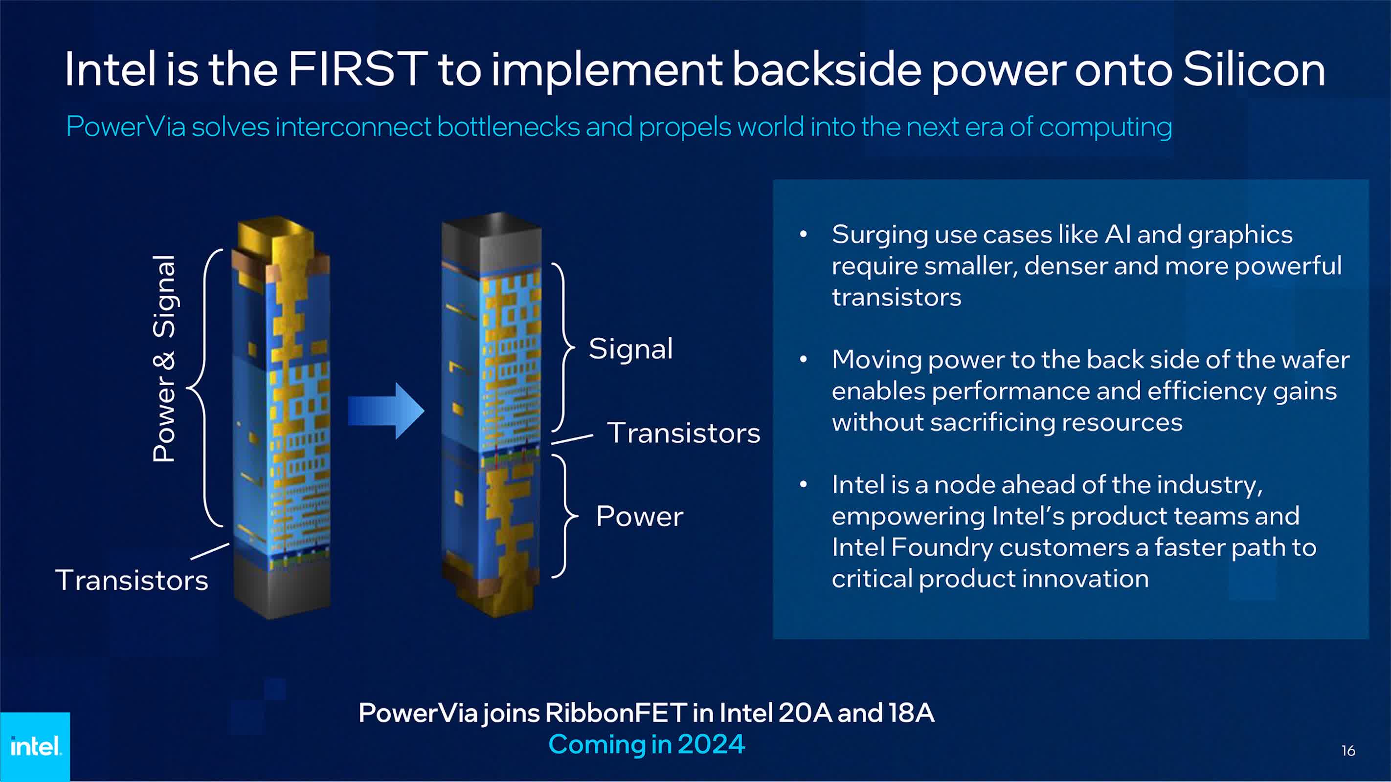
The technology's advantages are clear on paper. By separating power and signal paths, 18A reduces electrical interference and allows current to reach transistors more directly. That means higher clock speeds, lower voltage drops, and reduced heat – critical benefits as transistor scaling hits physical limits.
In theory, this gives Intel a lead of two process generations over competitors like TSMC, which doesn't plan to deploy a comparable system until the A16 process later in the decade.
But the same engineering leap that advances Intel's silicon also makes it hard to sell. According to an analysis by TechInsights, BSPDN represents a complete redesign of the chip's physical layout, forcing customers to rework established design methodologies from the ground up.
Existing toolchains, libraries, and workflows built for frontside networks can't simply be ported over. This divergence from conventional logic design is what limits external traction, even as Intel demonstrates Panther Lake's internal success.
The company's decision to push PowerVia ahead of the rest of the industry reflects a deliberate attempt to rebuild its technological credibility. Under former CEO Pat Gelsinger, Intel positioned 18A as the cornerstone of its foundry revival – a process node meant not only to compete with, but surpass, external foundry technology. Yet in doing so, Intel launched a manufacturing ecosystem that the rest of the design world hasn't yet caught up to.
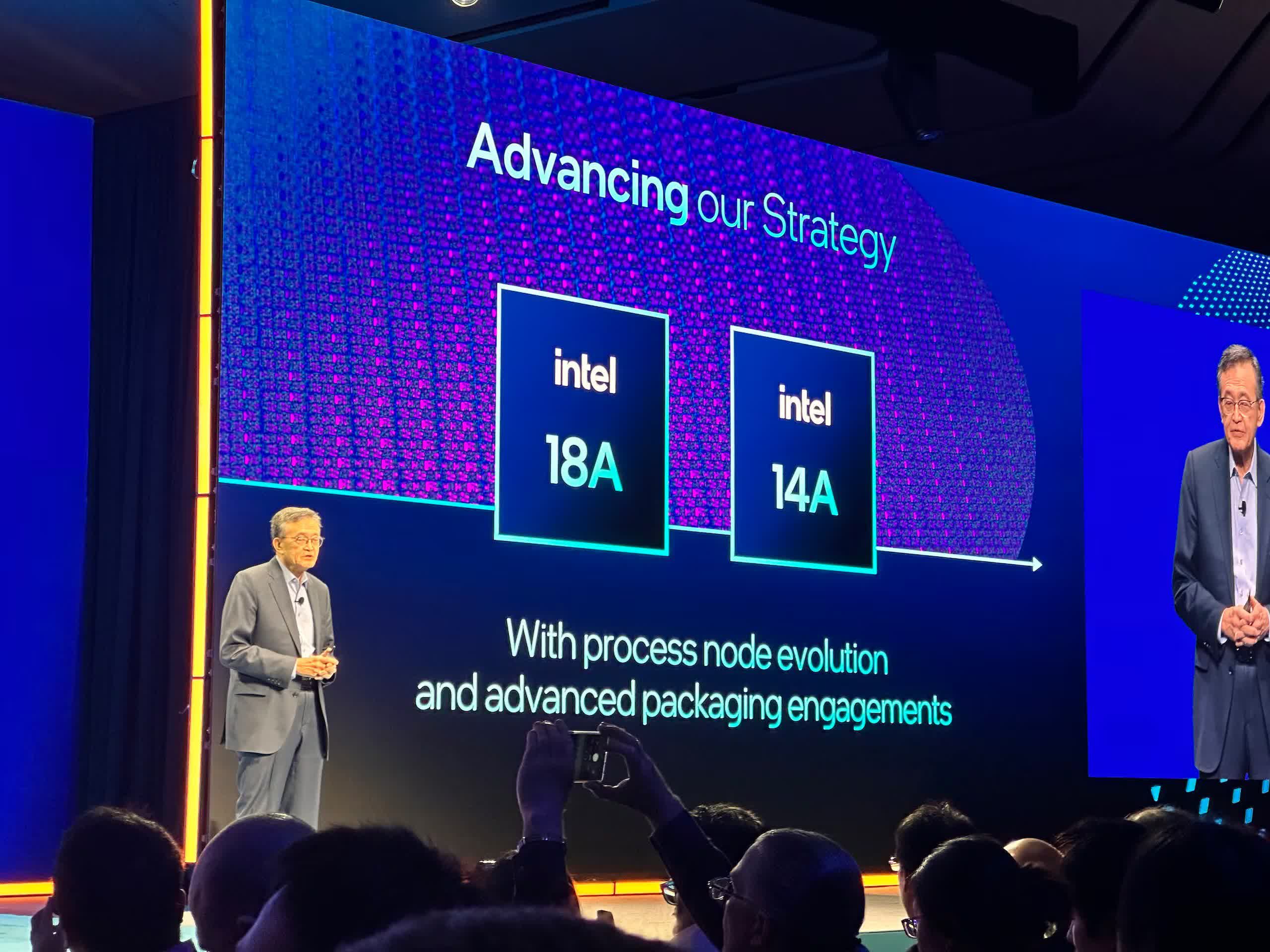
Analysts expect broader adoption of BSPDN later this decade, once tool vendors and design teams adapt to the new paradigm. Industry consensus points to around 2027 for wider uptake, which may coincide with Intel's next nodes – 14A and beyond – becoming more viable for external contracts.
By that time, PowerVia will have matured, and the costs of redesign may appear more justified against the gains in energy and compute efficiency.
For now, Intel has demonstrated that its 18A process works – and works well – but translating that success into foundry volume will take more than technical leadership. It will require convincing an entire ecosystem to rebuild its design habits from the backside up.