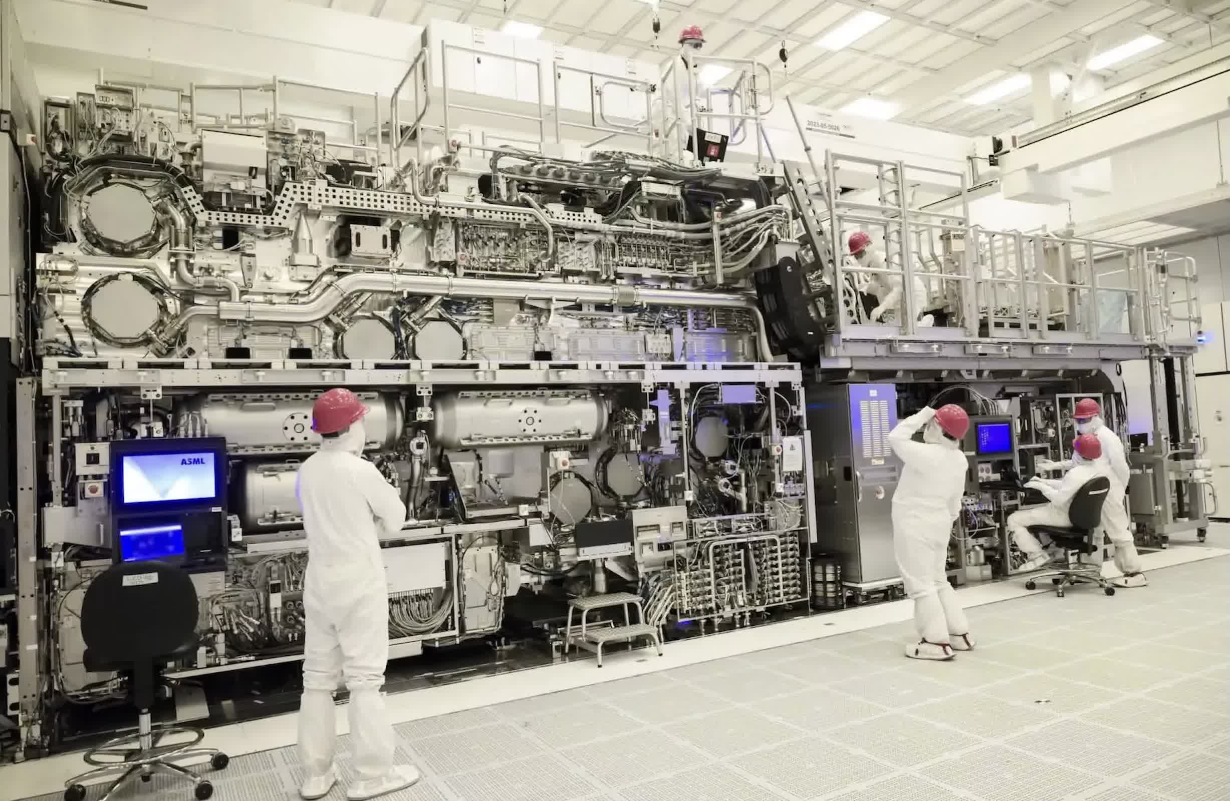
The big picture: In a laboratory near San Diego, ASML Holding's engineers have pushed the extreme ultraviolet beams generated inside the company's machines to a new threshold: 1,000 watts of continuous EUV power. The achievement is a technical milestone that could enable chip manufacturers to produce up to 50 percent more semiconductors per machine by the end of the decade, helping ASML maintain its dominant position in one of the most strategically important tech sectors in modern industry.
The achievement, confirmed by ASML technologists Michael Purvis and Teun van Gogh, does not involve a proof-of-concept demonstration or a short-lived experiment. The company says the new light source operates under factory-ready conditions and could be deployed in commercial systems later this decade. It represents a strong response to growing pressure from US startups and Chinese research programs seeking to replicate ASML's complex EUV process from the ground up.
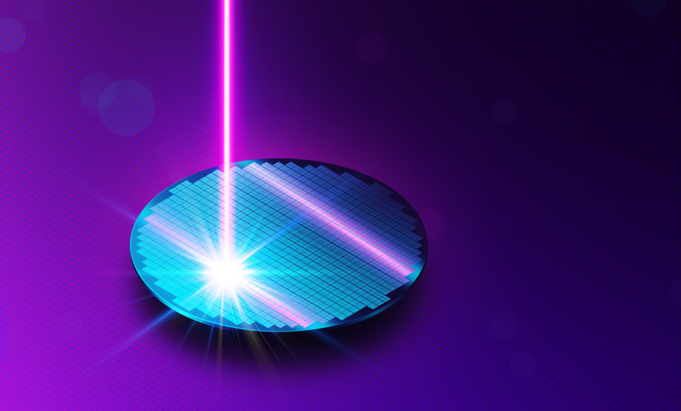
EUV, or extreme ultraviolet lithography, relies on light with a wavelength of just 13.5 nanometers – short enough to etch patterns only a few dozen atoms wide onto silicon wafers. To generate this light, ASML uses a precisely controlled sequence of events: a stream of molten tin droplets, ejected 100,000 times per second, is struck midair by a high-powered carbon dioxide laser. The collision vaporizes the tin into plasma hotter than the surface of the Sun, releasing EUV photons that are then captured by Zeiss-manufactured mirrors and directed onto the wafer.
Doubling the droplet frequency and introducing a second "shaping" laser pulse – rather than relying on a single pulse – proved critical to achieving the 1,000-watt output. The advance is compatible with the company's existing hardware architecture, Purvis told Reuters.
ASML's most recent production models process roughly 220 wafers per hour using 600-watt EUV sources. With the 1,000-watt systems planned for rollout before 2030, throughput could exceed 330 wafers per hour. Each wafer contains hundreds to thousands of semiconductor devices, depending on design complexity.
Shorter exposure times enabled by a more powerful light source also help reduce the overall cost per chip. "We'd like to make sure that our customers can keep on using EUV at a much lower cost," said van Gogh, who oversees ASML's NXE platform.
The development also advances the company's long-term objectives. ASML believes the design principles could eventually scale to 1,500-watt or even 2,000-watt light sources.
Such progress does more than improve chip yield – it also intensifies the global competition to develop alternative EUV manufacturing systems. ASML remains the only company capable of shipping commercially viable EUV lithography machines, a position that has prompted the US and Dutch governments to restrict technology transfers to China. Those controls, in turn, have accelerated Beijing's efforts to develop comparable systems domestically.
Meanwhile, American startups are advancing rapidly. Substrate and xLight have attracted hundreds of millions of dollars in private and government funding to develop what they claim could become next-generation lithography tools. In late 2025, the Trump administration announced up to $150 million in potential investment in xLight, signaling Washington's intent to support the development of a domestic alternative to ASML.
Even as challengers emerge, experts emphasize that the underlying physics remain extremely challenging. "It's very challenging because you need to master many things, many technologies," said Jorge Rocca, a laser physicist at Colorado State University whose laboratory has trained several ASML engineers. "What was achieved – one kilowatt – is pretty amazing."