Forward-looking: For years, the chip industry has chased better performance by shrinking transistors and squeezing more of them onto a flat slice of silicon. That strategy is running into hard limits. A group at the University of Illinois thinks the next gains will come not from going smaller, but from going vertical.
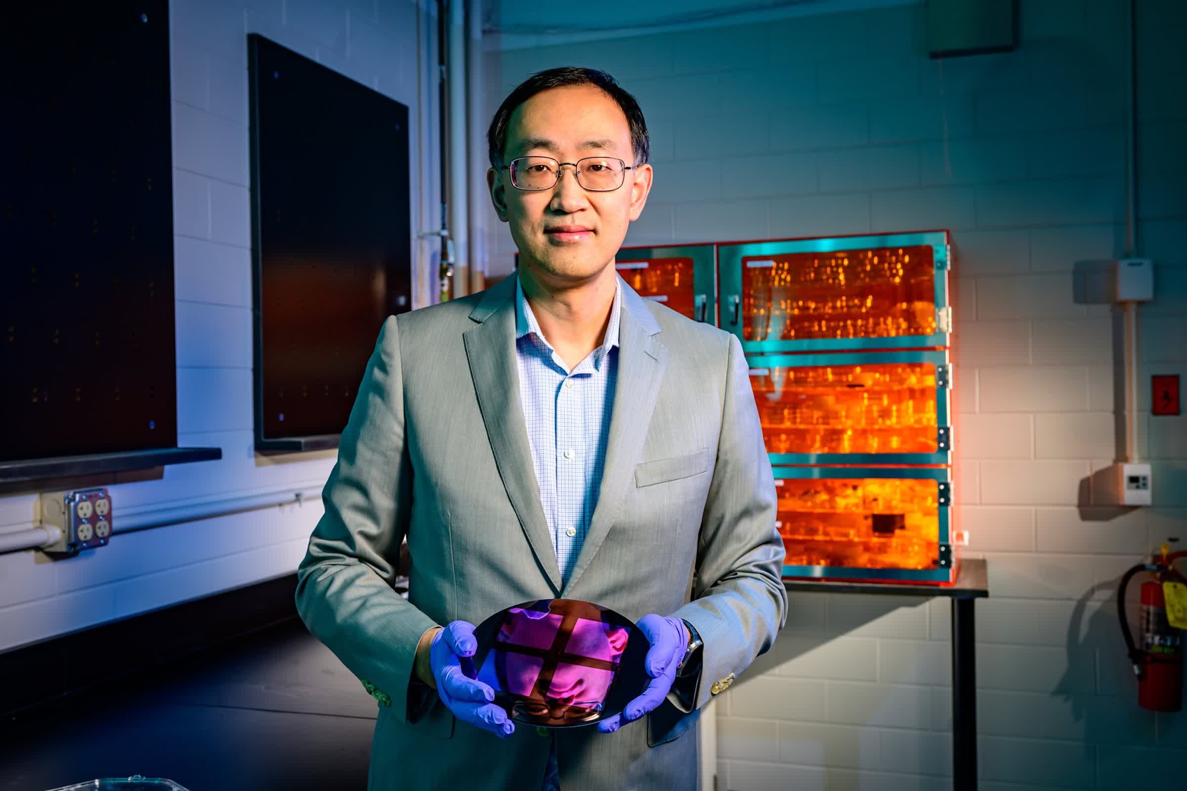
At the Grainger College of Engineering, materials science and engineering professor Qing Cao and his team have built working silicon circuits by stacking active layers directly on top of each other. Instead of adding more devices side by side, they are moving into the third dimension and building stacked layers on a single chip.
The push comes at a moment when traditional scaling is slowing. For roughly six decades, Moore's law has described an industry cadence where transistor counts and performance rise on a predictable schedule as features shrink. Now, that roadmap is harder to follow.
"In a sense, we're hitting a limit imposed by physics," Cao said. "If you look at the actual size of transistors, they're not getting smaller, especially in terms of their contacted gate pitch. This is because we're becoming limited by the intrinsic material properties of silicon and the fundamental rules of quantum mechanics."
Vertical integration offers a different way to raise compute density. By stacking logic and memory vertically, designers can shorten interconnect paths. That, in turn, increases bandwidth between blocks that would otherwise sit far apart on a flat die.
The idea of 3D chips is not new, and the market already has commercial products that stack silicon. High-bandwidth memory and AMD's 3D V-Cache both rely on bonding separate wafers or dies together. Those approaches, however, have limits in alignment precision and via density because they depend on relatively large through-silicon vias drilled between layers.
Monolithic 3D integration goes further. Each new layer is built directly on top of existing circuitry, which allows much finer vertical connections and tighter alignment.
The sticking point has been heat. Conventional high-performance silicon processing demands temperatures near 1,000 degrees Celsius. Once a first layer of metalized circuitry is in place, it cannot tolerate that kind of thermal load without damage. "Generally, the industry accepts that once the first layer of circuits is complete, the thermal budget limit for any additional layers is 400 degrees Celsius," Cao said.
Researchers have tried to dodge that problem by switching to other materials for upper tiers, but those devices have consistently lagged the base-layer silicon in speed and reliability.
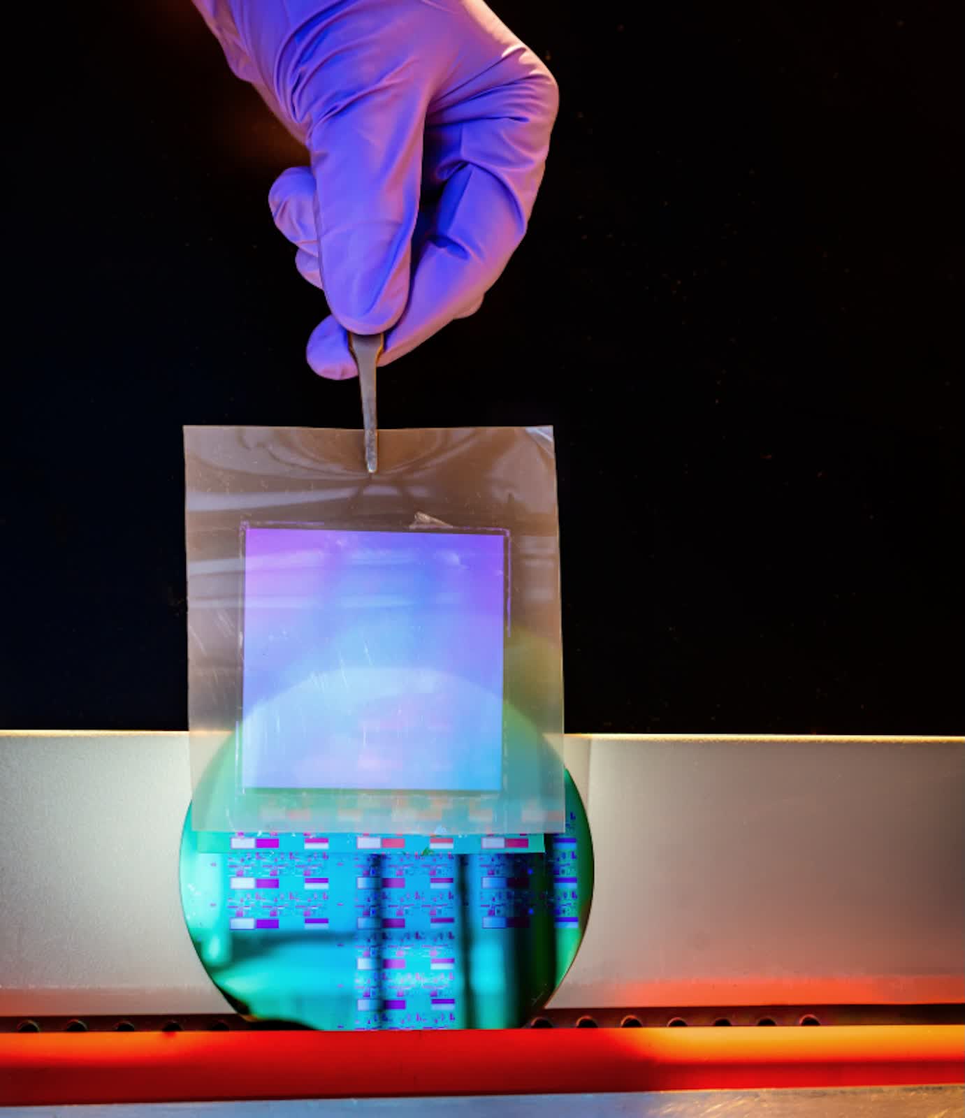
Cao's group stayed with single-crystalline silicon and instead changed how it is added. They start by making ultrathin freestanding silicon nanomembranes from a donor wafer. Those membranes are transferred onto a processed substrate using a roll laminator, at temperatures no higher than 200 degrees Celsius.
Because the membranes stay single-crystal, the stacked devices behave like conventional silicon transistors while still staying within the tight thermal limits for monolithic integration.

The physical form factor of the membranes helps as well. Cao noted that the team's approach is simpler and cheaper to put into practice, while also sidestepping some of the problems that come with traditional wafer stacking.
Instead of handling full-thickness wafers, they work with silicon membranes that are only about 10 nanometers thick, rather than the roughly 500 to 700 micrometers you see in a typical wafer. At that scale, the silicon becomes flexible enough to follow the contours of the layer beneath it, which helps the films sit snugly on the surface. That close fit reduces the risk of gaps and voids that often appear when engineers try to bond two rigid wafers together.
To stay within the thermal envelope, the team also rethought the transistor design itself. Traditional CMOS flows depend on doping steps carried out at high temperatures to define junctions. Instead, the group used junctionless transistors, where the silicon is heavily and uniformly doped before stacking. The ultrathin films still allow effective gate control, and the high doping levels help keep contact resistance in check.
On that basis, they built three stacked layers, each with 625 transistors, and wired them together with vertical metal interconnects. The devices showed strong uniformity and high yield, and their output current densities matched those of standard silicon transistors produced on bulk wafers at much higher process temperatures. They also outperformed monolithic devices built from alternative materials by at least a factor of three to four. The team used the stack to implement three-dimensional logic and static random-access memory cells.
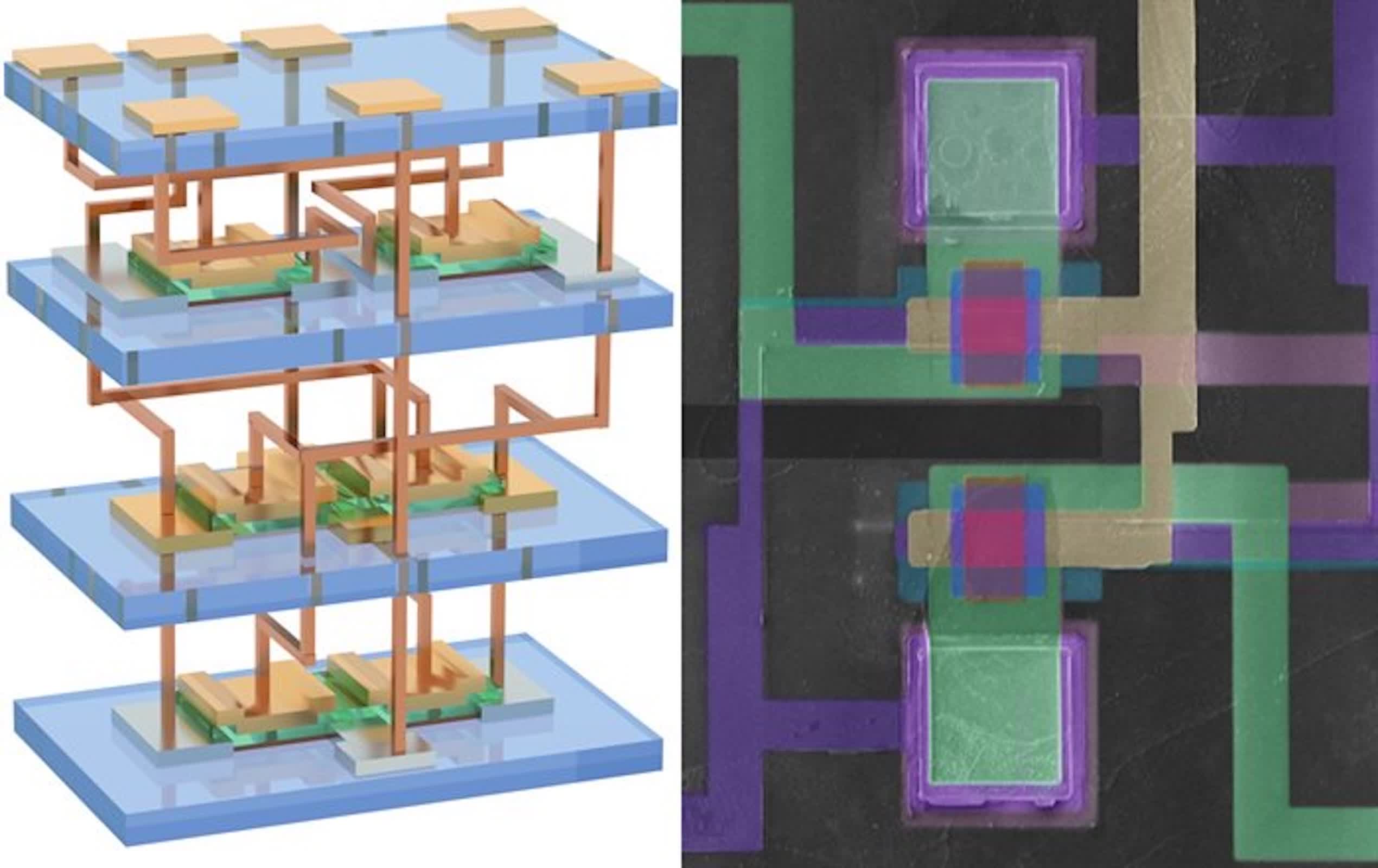
SRAM illustrates the architectural impact. "Take something as simple as static random-access memory, which is universal in CPUs and GPUs. Today it takes six microelectronic devices called transistors on a single plane to store one bit of information.
With vertical integration, you can distribute them across multiple layers. It's like replacing a sprawling suburb with high-rises: you get the same functionality, but the spatial footprint is reduced while making communication between layers faster and more efficient," Cao said.
The group is positioning this as a path toward manufacturing rather than just a lab curiosity. Reported device yields are in the 98% to 100% range. "For the first time, we have met the thermal budget of monolithic 3D integration using standard single-crystalline silicon and delivered unprecedented performance," Cao said.
Cao emphasized that the key outcome of the work is that the process can be scaled up, not just shown in a one-off lab demo. In principle, more layers can be added on top of the three the team has already built, while still delivering fast, consistent transistors with strong yields and limited variation from device to device. In his view, that puts the group in a good position to hand the technique off to a commercial foundry and show that it can translate quickly into real-world semiconductor manufacturing.
The project ran through Illinois Grainger Engineering's Center for Advanced Semiconductor Chips with Accelerated Performance, which counts IBM, Intel, and TSMC among its partners. The researchers are now preparing to move the technology into an industrial foundry, a key step if monolithic 3D silicon chips are going to show up in commercial systems rather than just in research papers.