The big picture: Samsung's upcoming 3nm-class lithography process will be their first to use gate-all-around (GAA) transistor technology. In the face of concerns raised about if the company will have GAA designs out in time to keep pace with competitor TSMC, it insists that its first iteration of the technology will begin mass production in 2022.
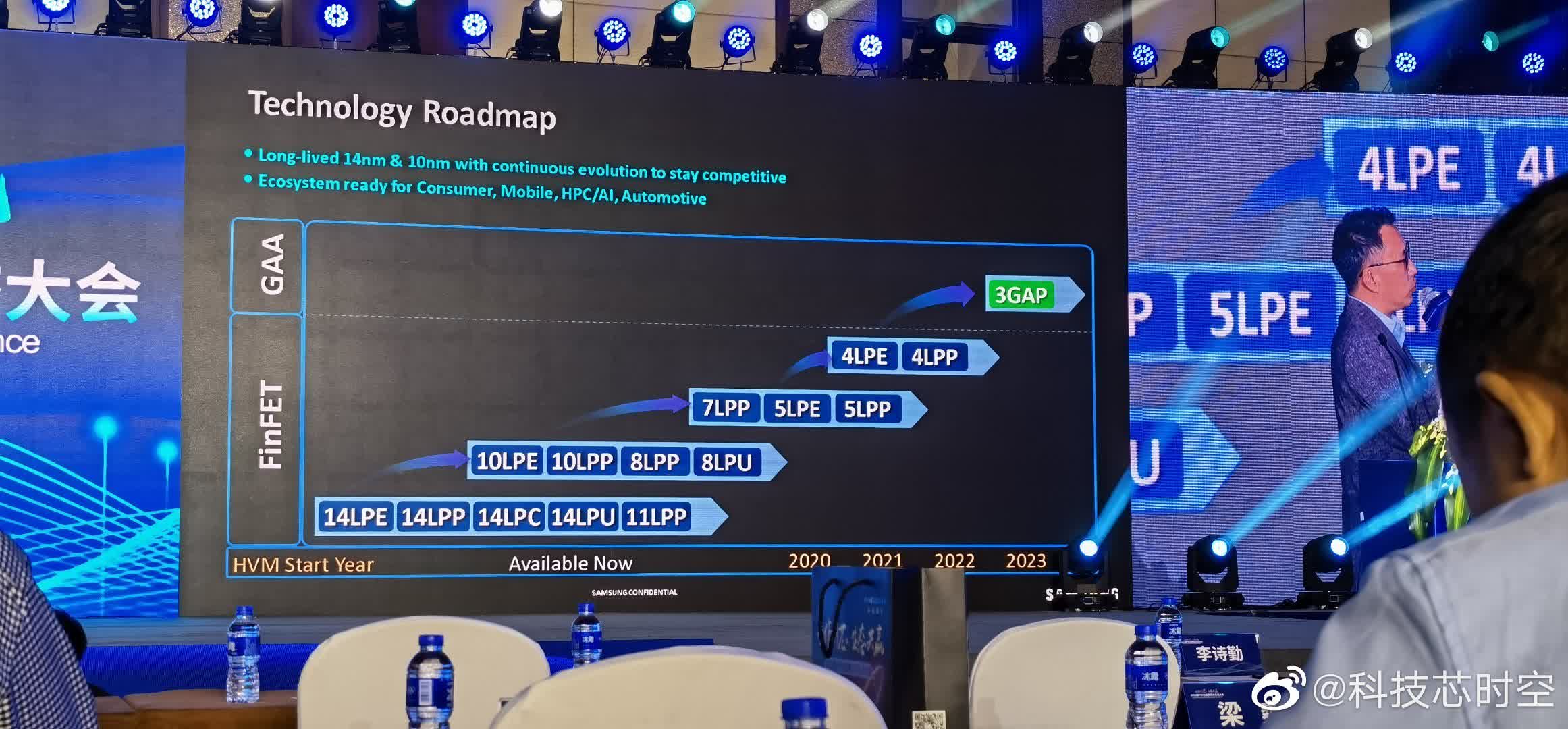
Samsung's public roadmap was presented recently at its Foundry Forum 2021 in China. Particularly conspicuous in its absence from the slide shown however was Samsung's 3GAE (3nm, GAA-Early), the first iteration of their 3nm technology. 3GAE was originally revealed in 2019 alongside its follow-up, 3GAP (3nm, GAA-Plus), but only the latter was shown off in the presentation.
Prior to this roadmap being revealed, there had already been concern brewing over the health of the node; 3GAE had originally been planned for risk production in late 2020 and volume production in 2021, but the company only taped out its first 3nm test chips last month.

Furthermore, Dr. Chidi Chidambaram, VP of Engineering at Qualcomm, Samsung Foundry's largest third-party customer was quoted by SemiAnalysis as estimating GAA technology as only reaching production in 2023-24, at a recent event hosted by Applied Materials.
While the estimate is likely intentionally vague for NDA reasons, it still puts Samsung a year behind TSMC's plans for volume production of 3nm-class silicon next year. This, combined with the absence of 3GAE on the published roadmap, led to speculation that the node had been completely skipped over in favor of 3GAP.
Just to explain the naming by Samsung: 3GAE (Gate-All-Around Early) is missing here. This indicates that the early process is not viable for mass production and got killed completely. 3GAP (Gate-All-Around Plus) now planed for HVM in 2023, which is confirming Qualcomm's statement https://t.co/9GeMcLq3jt
--- Andreas Schilling (@aschilling) July 7, 2021
When contacted for comment by Anandtech, the company said that 3GAE was still due for mass production in 2022, and it's possible that the node isn't being publicized simply because it's reserved for internal usage at Samsung LSI.
However, while this was done with other "-Early" process variants from the company in the past, those were still marked on the map; 5LPE saw third-party usage in Qualcomm's Snapdragon 888, but that node was itself derived from 7LPP.
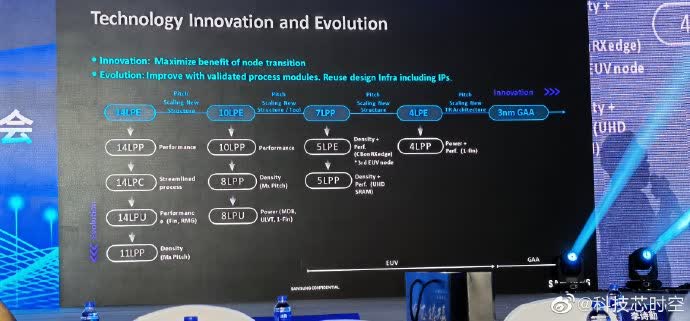
The company is also putting out a 4LPP, based on more traditional FinFET technology. This (and its predecessor 4LPE) are now listed as their own family of nodes, instead of being an evolution from 5nm/7nm-class technologies.
It may be that the process has a substantial enough improvement to warrant marketing as a new "headline" node, or simply because of more significant differences in design and manufacturing.

Still, the absence of 3GAE on the public roadmap and the FinFET-based 4LPP node overlapping with Samsung's stated 2022 target for 3GAE draws uncomfortable comparisons with Cannon Lake, Intel's earliest 10nm processors.
Those technically shipped in 2018 to meet investor commitments, but were so bad that they were passed over in favor of further evolutions of the older 14nm node; the company now ignores that generation completely, insisting that Ice Lake was its first real 10nm line-up.
But, perhaps, at least the oft-mocked 14+++ was more easily understandable than a branching tree of processes and their sub-evolutions.
