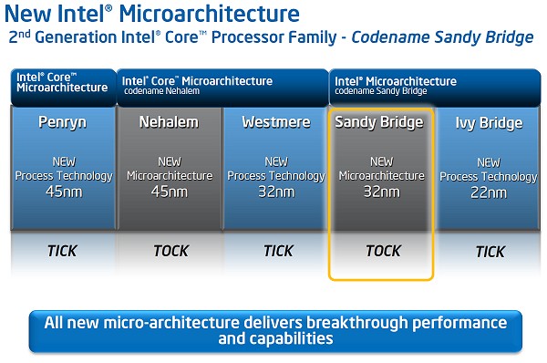
From Clarkdale to Sandy Bridge
The current crop of 32nm "Clarkdale" Core i3 and Core i5 processors are exclusively dual-core, meaning that in order to support 4 threads they must rely on Hyper-Threading. Sandy Bridge on the other hand will offer both dual and quad-core processors, though not all will support Hyper-Threading technology.
L3 cache support in Clarkdale CPUs was limited to 4MB. The Sandy Bridge architecture differs, though things are a little more confusing. The Core i5 range will provide a 6MB L3 cache, while the Core i7 processors will receive 8MB L3 cache. The more affordable Core i3 range will be cut down to a 3MB L3 cache.
However the Sandy Bridge architecture features a shared L3 cache that is shared across all cores and the processor graphics as well. Intel claims that this shared cache design delivers more performance and greater energy efficiency.

A problem with the Nehalem architecture was that regardless of how many cores the processor had (two, four or six), each individual core had its own private path to the L3 cache. This makes the processor considerably more complex and becomes a larger issue when adding more cores. It's said that each core required around 1000 wires and when adding a GPU to the equation even more wires are required.
Sandy Bridge adds a GPU and video transcoding engine on-die that share the L3 cache. Rather than laying out another 2000 wires to the L3 cache Intel introduced a ring bus. The ring features four separate rings: data, request, acknowledge and snoop. Each core, the graphics processor, the video transcoding engine and system agent all have their own stop on the ring bus.
For those of you who are wondering what the system agent is, it's essentially the on-die North Bridge. Previously Intel has coined this as the un-core, but for some reason it is now titled system agent. Regardless everything is much the same in terms of features, as you get a single PCIe 2.0 x16 lane which can be split into dual x8 lanes when using multi-GPU technology.

The dual-channel DDR3 memory controller has been improved as it falls back on the Lynnfield design. Whereas Clarkdale moved the memory controller off the CPU die and onto the GPU, it is now back on the CPU die with the Sandy Bridge architecture.
Another major change has to do with the DMI interface between the processor and the Platform Controller Hub (PCH) otherwise known as the chipset. The LGA1156 processors communicate to the PCH using the DMI interface which provides a bandwidth of 2GB/s. Because the PCI Express 2.0 x16 lanes and the DDR3 DIMM slots are connected directly to the processor, the limited 2GB/s bandwidth was never a problem.
However with the introduction of SATA 6Gb/s and USB 3.0, more bandwidth between the CPU and PCH will be required. Therefore Intel has upgraded to the DMI 2 interface, which provides four PCI Express 2.0 x1 lanes for a maximum theoretical bandwidth of 2GB/s in each direction, for an aggregate of 4GB/s.

Also new to Sandy Bridge is the Intel Advanced Vector Extensions (AVX) which is the latest expansion of the Intel instruction set. It extends the Intel Streaming SIMD Extensions (SSE) from 128-bit vectors into 256-bit vectors. Intel AVX addresses the continued need for vector floating-point performance in mainstream scientific and engineering numerical applications, visual processing, recognition, data-mining/synthesis, gaming, physics, cryptography and other areas of applications.
The enhancement in Intel AVX allows for improved performance due to wider vectors, new extensible syntax, and rich functionality including the ability to better manage, rearrange, and sort data.