Serving tech enthusiasts for over 25 years. TechSpot means tech analysis and advice you can trust.
When you buy through our links, we may earn a commission.
The modern graphics processor has become one of the largest, most complex, and most expensive components found in almost any computing device. From the early VGA days to the modern GPU. The history and evolution of the chip that came to dominate gaming, and later AI and compute.
By 2013, each of these companies was following a similar architectural design path, with their products primarily targeting PCs and workstations. This trend was largely influenced by the evolving nature of rendering, the requirements set forth by graphics APIs, and the expanding use of GPUs in computing and AI applications.
However, in the years that followed, graphics processors evolved to become one of the largest, most complex, and most expensive components in a wide range of computing devices.
...in the years that followed, graphics processors would become one of the largest, most complex, and most expensive components that could be found in almost any computing device.
Something old, something new, plus a nice lawsuit to boot
In 2014 we saw new architectures released by most of the major vendors, as well as a slew of products using older technologies. In the case of AMD, their line-up consisted of almost entirely previous systems. In the desktop market, we were given models using Graphics Core Next (GCN) 1.0 and the even older TeraScale 2 architecture. A good example of the former was the Radeon R9 280, released in March.
This was a rebranded Radeon HD 7950, from two years earlier, but at least AMD had the sense to launch at a lower price compared to its first iteration. Not long after that product, GCN 2.0-powered Radeon R9 295X appeared and it was very the polar opposite to the 280.
Old tech, doubled up, gave surprising results
Sporting two GPUs, a custom water-cooling system, and a price tag of $1,499, it jumped straight to the top of the performance tables, and we were pleasantly surprised at how good it was (despite its staggering cost).
In September 2014, AMD released the Radeon R9 285 – this card sported a new chip, with a refresh of their GCN architecture, that brought minor improvements in the cache and tessellation systems to the table. At $250, it was pitched at replacing the old R9 280, and came with higher clocks all round. It was only marginally faster, though, due to having 25% less memory bandwidth.
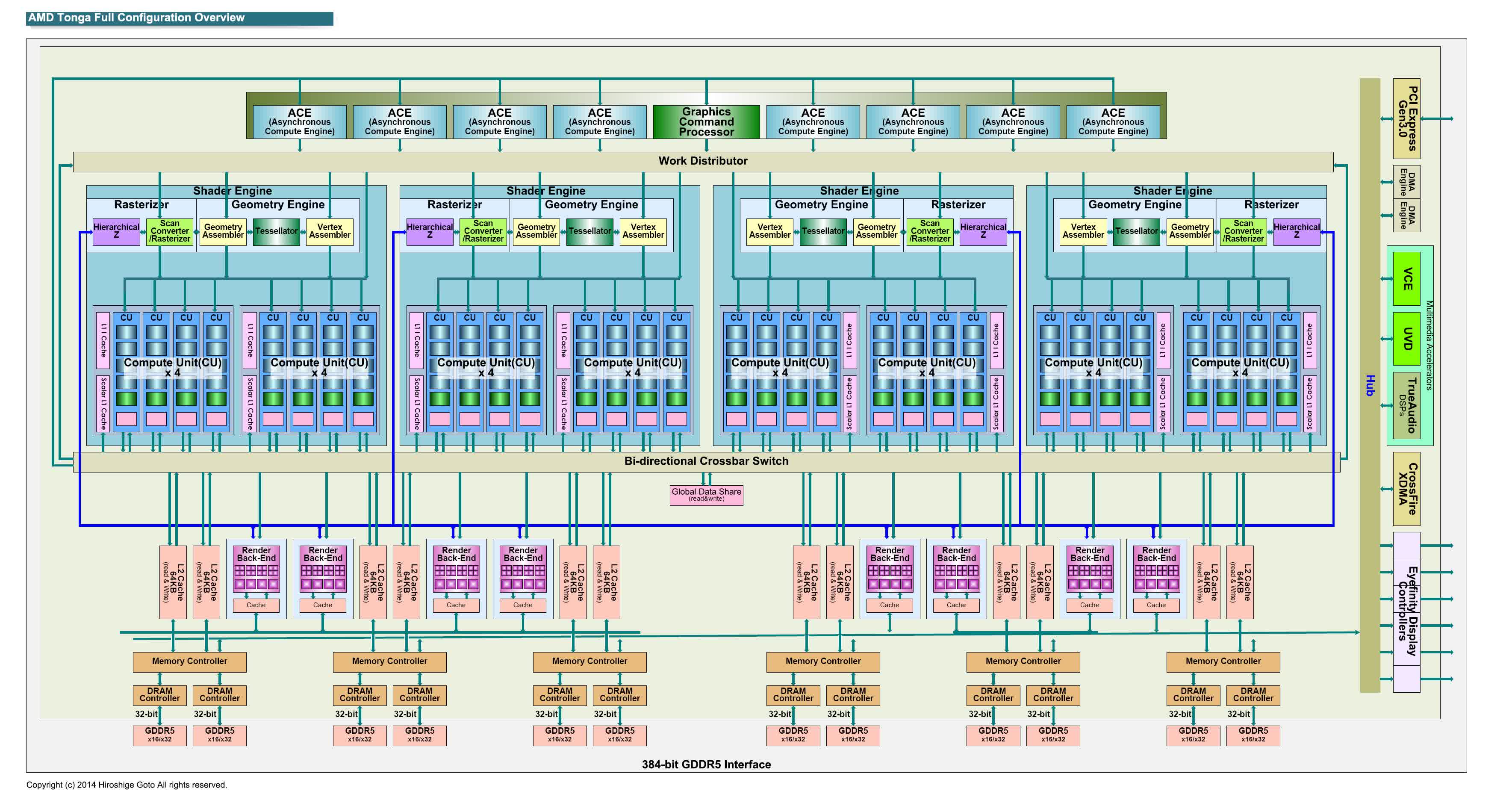
The layout of AMD's first GCN 3.0 GPU – the R9 285 had four memory controllers disabled. Image: PC Watch
It might seem odd that AMD made such little progress with GCN 3.0 but at the time, they were struggling with large debts and poor levels of operating income; to combat this, they focused on more profitable markets, such as low power systems and semi-custom designs.
In contrast, Nvidia's fortunes were largely buoyant that year. They made a steady gain in both revenue and net income, despite some odd decisions about products. Like AMD, they used older systems, refreshed ones, and a new architecture (Maxwell) – in the case of the latter, it wasn't used in a top-end, halo model, but instead came to light in a $150 mid-range offering.
Not the most inspiring choice to highlight a new GPU architecture
The GeForce GTX 750 Ti was designed to compete against the likes of AMD's Radeon R7 265. Despite the new tech, it generally wasn't as fast as the Radeon. Had that been all Nvidia offered in February 2014, one might have thought they were losing momentum.
This was compounded because to no fanfare whatsoever, Nvidia refreshed their best-of-the-best line – the GeForce GTX Titan – with the simple addition of the word 'Black' and a slightly higher clock speeds. At $999, it was no more expensive than its forefather, but it was hardly making the news headlines.
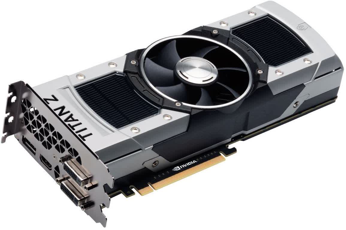
To combat AMD's Radeon R9 295X2 launch in April, Nvidia brought out the Titan Z in the following month. As an exercise in pure hubris, it garnered huge amounts of attention for all the wrong reasons.
King Kong size, Godzilla price, Mr. Magoo performance
Hardly any samples were issued to reviewers to analyze, and none were willing to personally shell out for the $2,999 asking price. For the few that did manage to test it, the overall performance was less than ideal for such an expensive product – generally worse than the the R9 295X2 and two of Nvidia's older GeForce GTX 780 Ti cards in SLI.
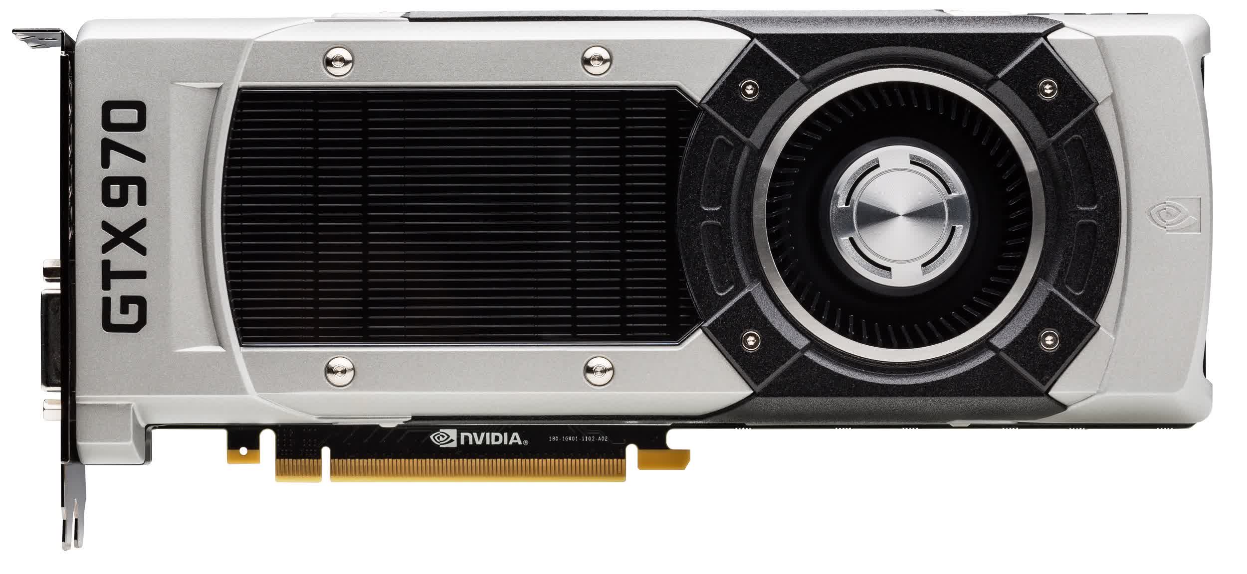
Matters greatly improved in September, when the GeForce GTX 900 series arrived in stores, even though only two models were available.
The GeForce GTX 980 and 970 sported Maxwell-based chips, albeit with minor tweaks, and went on to grab numerous headlines. The first of which were about the prices: at $529 and $329 respectively, the new models were both cheaper than the GTX 780 and 770 at launch. Performance was good, being competitive against AMD's offerings and Nvidia's own back catalogue.
All in all, it should have been a successful end to the year for Nvidia, but the GTX 970 was hiding a 'feature' that would rapidly undo all of the good press that the launch of the new series had accrued.
The model's specification sheet stated that it had 4 GB of 7 Gbps GDDR5 memory on a 256-bit bus – to all intents and purposes, the same as on the GTX 980. The details tied in with the claim that the GPU sported 64 ROPs (render output units) and 2 MB of L2 cache.
However, what Nvidia kept quiet about was that this wasn't entirely true – it only had 56 ROPs and 1.75 MB of L2 cache, which meant that the memory bus should have only been 224-bit and thus only of 3.5 GB of RAM. So where was the other 0.5 GB?
It really was there, so it was "4 GB on a 256-bit bus", but not in the same manner as in the GTX 980. Due to the configuration of crossbar ports and memory controllers, the system could read/write in parallel across the 224-bit connection to the 3.5 GB or use a single 32-bit bus for the remaining 0.5 GB.
With a L2 cache block disabled in the GTX 970, access to the last 0.5 GB was heavily penalized
As news of this apparent deception came to light, Nvidia scrambled to explain the situation, blaming it on errors in the publishing of their documents for the press.
They provided an explanation for the setup (as detailed in the above image) and apologized for the mistake, pointing out that the ROP+memory configuration wasn't actually a problem, and was fully intentional. But the damage was done, and two years later, they were forced to offer compensation to numerous class action lawsuits, and publicly offered $30 to all GTX 970 purchasers.
Intel also released a new architecture during 2014, codenamed Gen8, as a core part of their Broadwell-range of CPUs. Integrated GPUs almost never garner any interest, despite being such a significant portion of the CPU die, but the design marked some notable improvements over its predecessor.
A Core i5 was more GPU, than CPU, in 2014
Both pairs of SIMD (single instruction, multiple data) processors in the EUs (Execution Units) could now handle integer and floating point operations, whereas it was just the one previously. The effective doubling of the integer throughput rate was matched by providing support for FP16 data formats – again, at a doubled rate.
These changes brought the tiny GPUs in touch with the architectural capabilities of AMD and Nvidia chips – however, the paucity of EUs, texture units, and ROPs still made them unsuitable for gaming.
Not that small GPUs aren't capable of running decent looking games...
In the smartphone world, Apple launched the iPhone 6 in September, powered by their internally designed A8 SoC (system-on-a-chip). This processor used licenced CPU and GPU structures from Arm and PowerVR, but the latter also contained some custom units made by Apple themselves.
Apple was debuting their new Metal API. This collection of libraries included graphics and compute shaders, all heavily optimized for the GPUs in iPhones and iPads. As developers became more familiar with the software over time, it gave Apple's products a distinct performance advantage over the competition.
The need for better programming control and low-latency libraries wasn't just restricted to smartphones. Behind the scenes, the Khronos Group (a consortium of industry bodies) began work on creating the successor to OpenGL – the aim being to provide a cross-platform graphics and compute API, based on AMD's work with their Mantle software.
And software was to become a critical feature of the following year.
Something old, something new... wait, this again?
In many ways, 2015 was just a repetition of the prior year. AMD launched nearly 30 different graphics cards, with the large majority of them using the old GCN 1.0 or 2.0 architectures.
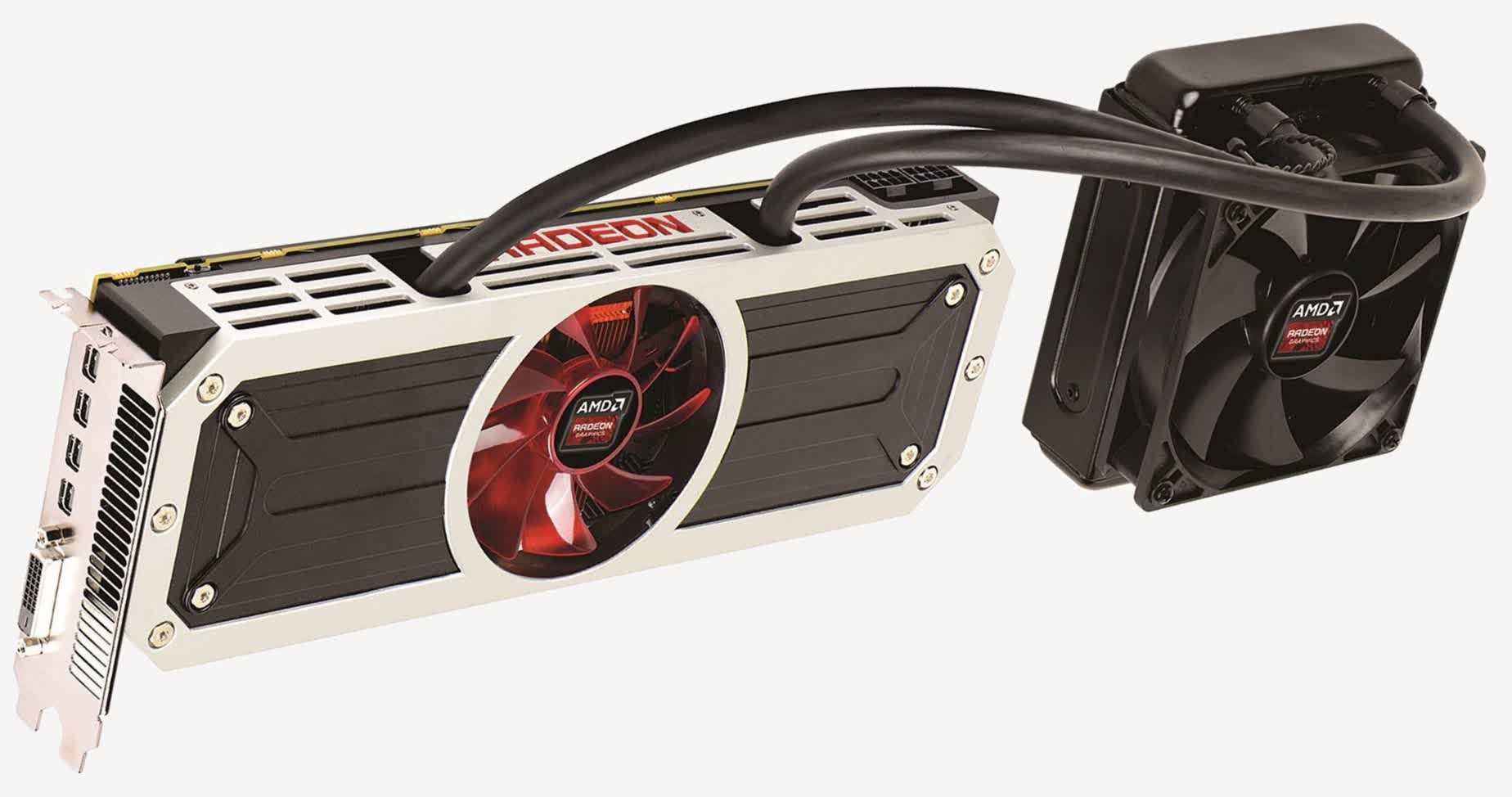
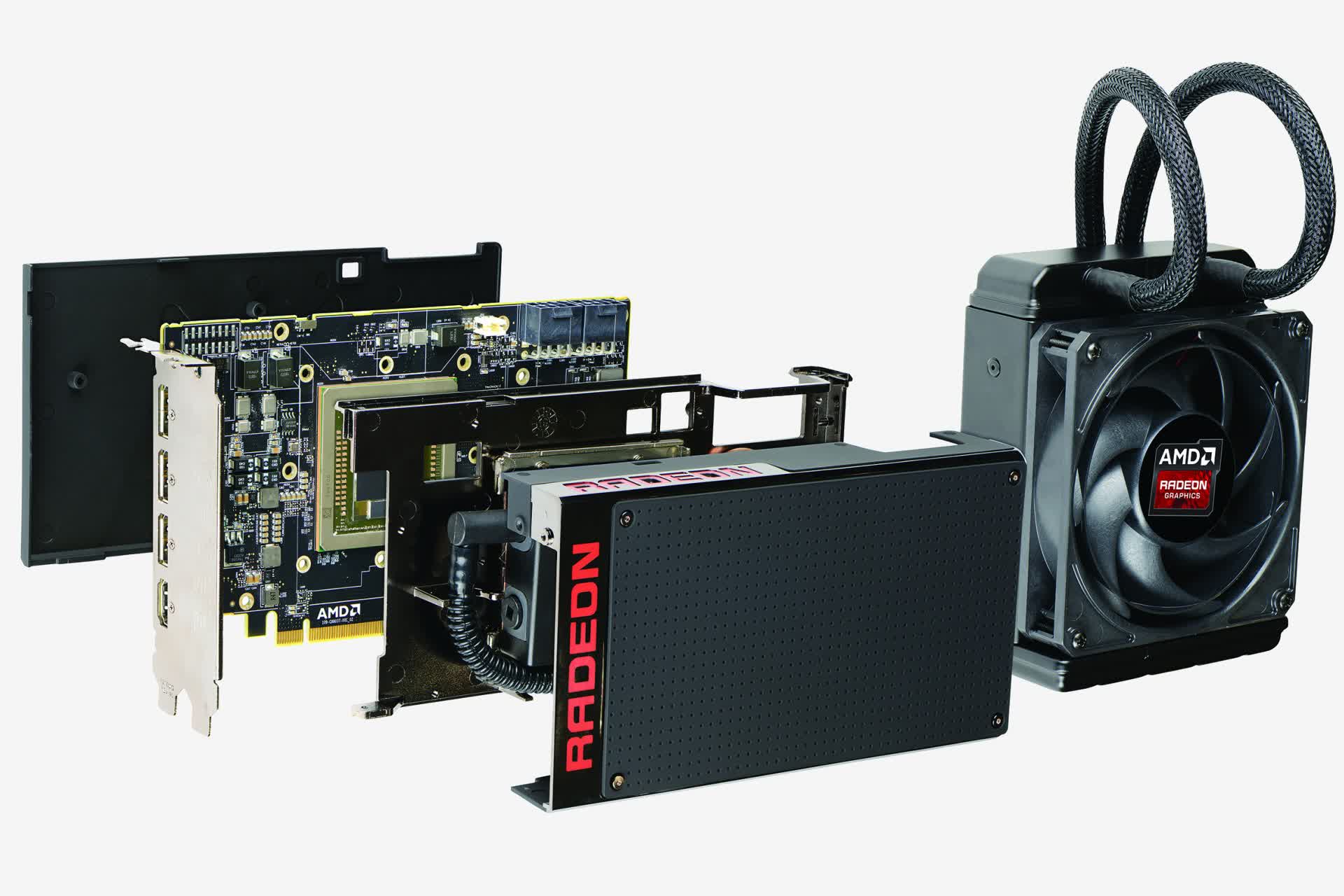
The silicon chip veteran took a shotgun approach to the scheduling of product releases, though. In June, just one week separated the appearance of the GCN 2.0 powered Radeon R9 390X (essentially a single GPU R9 295X2, with a clock bump) and the brand-new Radeon R9 Fury X.
Although there was a $200 difference between the two, the more expensive Fury could justify that price. The 596 mm2 GPU, codenamed Fiji, packed in an astonishing 4096 shader units – 45% more than the 390X. It was also the first consumer-level graphics card to use HBM (High Bandwidth Memory).
A tiny graphics card with a massive GPU – it has to be the Radeon R9 Fury X
This technology involves stacking the DRAM chips on top of each other and running the interconnects through them. The end result being a far more compact system that provides lots of memory bandwidth, albeit with no more than 4 GB of it in total, for the first iteration.
But all those shaders and fancy new RAM came at a cost – both literally and figuratively. The peak power consumption was high (though no more so than the R9 390X) and AMD's design had issues with temperature. Thus the Fury X was sold with an integrated water cooling setup, that turned out to be very effective.
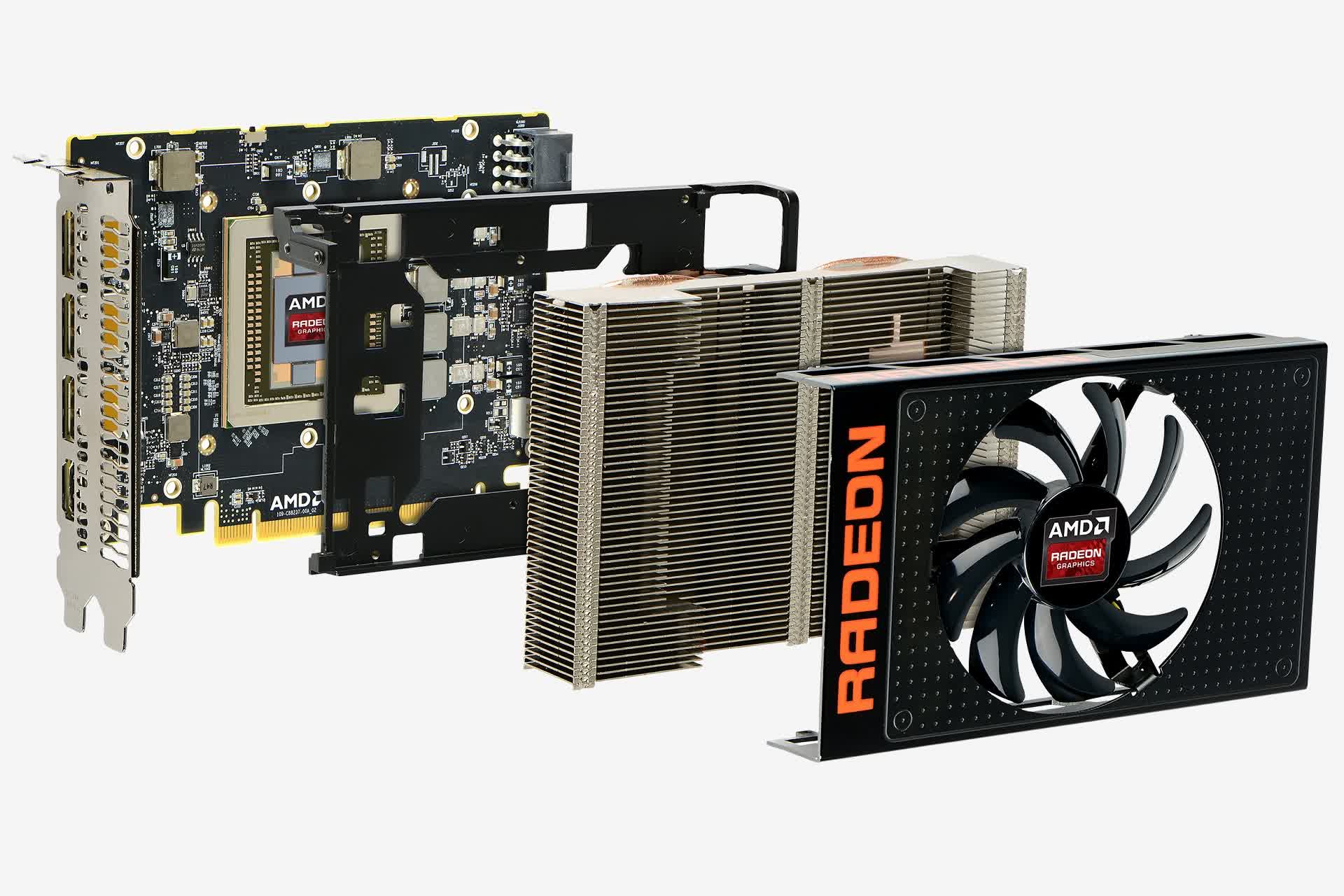
The non-X version ran just about cool enough to not require it, due to having lower clocks and 8 Compute Units disabled, and all third party variants of the model used traditional heatsink and fan combinations. As did the Radeon R9 Nano, AMD's baby version of the Fury X, that came to market a month later.
The R9 Nano – less heat, smaller size, same price as the Fury X
The Fiji-line of graphics cards were AMD's best performing by a large margin and despite the price tag, heat, and comparatively small amount of memory, it sold extremely well. It would come to face stiff competition from Nvidia, even though they generally had a relatively low-key first half to the year, with respect to exciting new products.
Something else that AMD brought out in early 2015 was FreeSync – a royalty-free alternative to Nvidia's proprietary G-Sync (read our 2021 take). Both were variable refresh rate systems that allowed monitors to remain synchronized to frame updates, reducing the problem of screen tearing, without locking the rate of changes in place.
Radeon GPUs had featured the ability to do this for a while, whereas GeForce chips at the time required an external device to be built into the monitor.
For Nvidia, the majority of their releases were budget and mid-range models, with the most notable being the GeForce GTX 960, making an appearance at the start of the year. At just $199 and using 120 W, it was a better demonstration of the progress Nvidia had made with the Maxwell architecture.
The GM204 GPU was essentially the same as that in a GeForce GTX 980, but sliced in two
Performance-wise, it was on par with the likes of the Radeon R9 280 and 280X, and a little cheaper. This was entirely down to the difference between the chips used in the competing products – the GTX 960 housed a 228 mm2 GPU, comprising 2.94 billion transistors, whereas AMD's older models used 432 mm2 chips, with 4.31 billion transistors.
Despite both being manufactured on TSMC's 28 nm process node, the newer architecture highlighted how much progress had been made since GCN 1.0 first appeared.
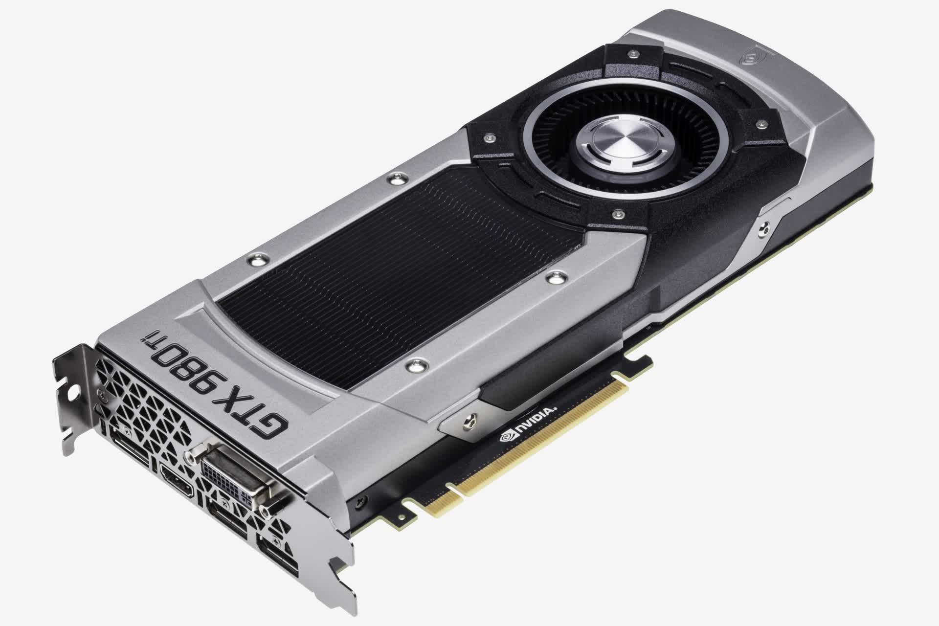
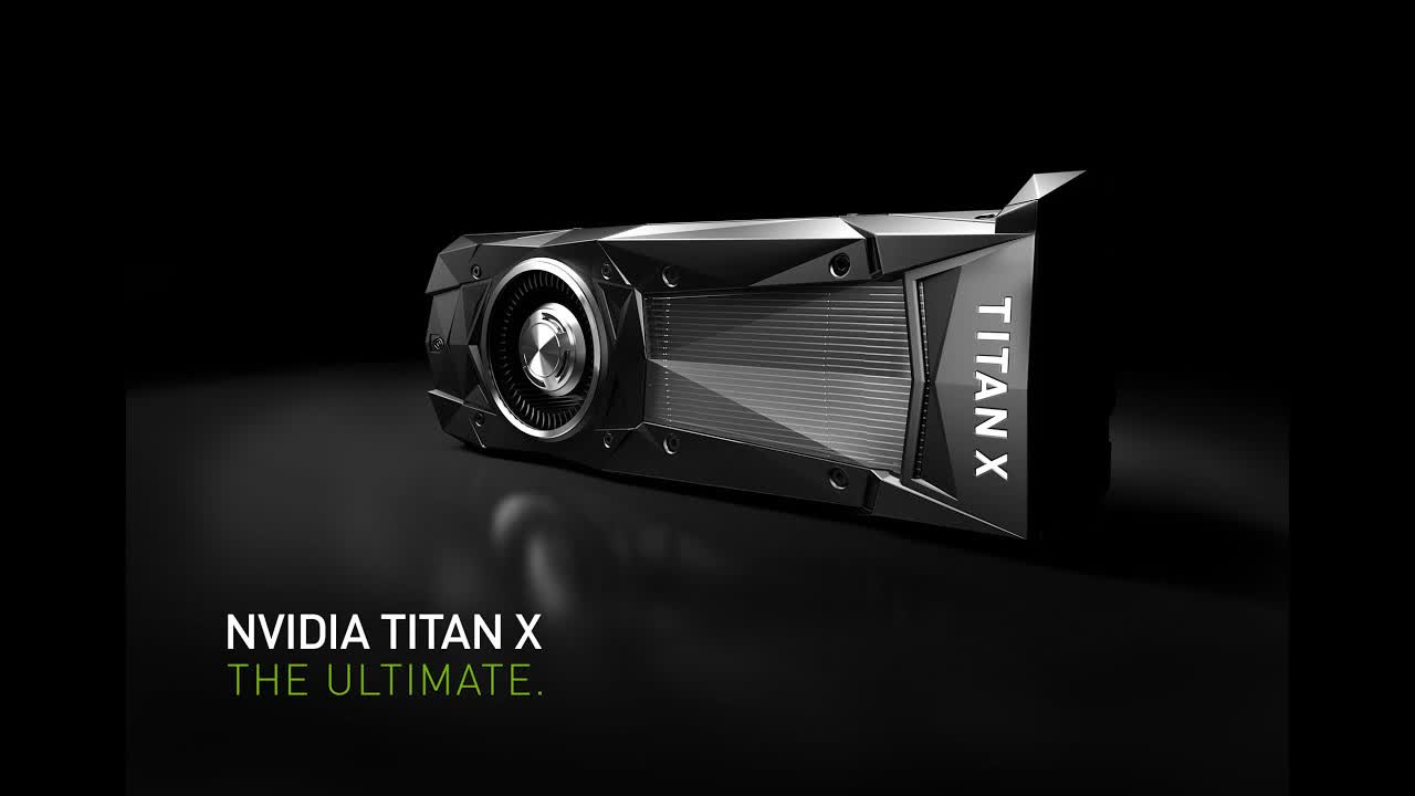
At the other end of the GPU scale, Nvidia only offered two new models and both used the same GM200 chip. The GeForce GTX Titan X launched in March and the GeForce GTX 980 Ti in June. With a price tag of $999, the former was targeted at a very niche market, but the 980 Ti was launched at $649 – still very expensive, but far more palatable to a wider audience.
The Radeon R9 Fury X had yet to appear, and Nvidia's top graphics cards were being pitched against the likes of the R9 295X2 and 290X. Depending on the game, they offered better performance, although AMD's models were far more cost-effective.
2015 also saw software releases and announcements that would go on to shape the direction that GPUs and their vendors would follow for their forthcoming architectures. In March, at the annual Games Developers Conference, the Khronos Group publicly named the project they were working on: Vulkan became a hot topic.
This new graphics API was offering significant benefits over OpenGL and Direct3D, mostly in the form of transferring a lot of the management of memory, threads, and the GPU itself to the developers and away from GPU drivers. This would help to greatly reduce the CPU overhead that the systems in place at the time were struggling with.
Four months later, Microsoft launched Windows 10 and along with it, DirectX 12.
The graphics portion of this API called Direct3D offered similar features as Vulkan, although it was restricted to the new operating system only – users with older versions of Windows were forced to remain with DirectX 11.
Not that it had the best of promotional starts, though. The first DirectX 12-only game was, naturally, a Microsoft one – Gears of War: Ultimate Edition. The title was a catastrophic mess, with numerous bugs and dire performance. Other games using the new API were to appear in the following year, but it would take longer for the software to reach its full potential.
One of its features, asynchronous compute, was of particular interest to developers. Compute shaders had been a part of DirectX for a while, having first appeared in DX11 in 2008 (and via extensions in OpenGL and Nvidia's CUDA software). Handled specifically by the API DirectCompute, these shaders ran on a separate pipeline to the graphics one (e.g. vertex, geometry, pixel shaders) and leveraged greater general purpose computing ability to a GPU.
Switching between the pipelines typically resulted in a performance penalty, so the ability to execute both at the same time with asynchronous compute, was potentially powerful. However, despite both AMD and Nvidia claiming their latest architectures were DirectX 12 compliant, only AMD's GPU made best use of the feature – Nvidia's Maxwell chips weren't designed to operate in this manner particularly well.
Before the year closed, Google shifted their TensorFlow software to open source, giving the public full access to the library of artificial intelligence and machine learning tools. While it wasn't the first of its kind, Google's efforts that year were matched by Intel (with DAAL), Microsoft (CNTK), and Apache (MXNet).
Graphics cards were already in use for such roles (AI, ML), but the increasing demand for massively-parallel compute ability would come to dominate how GPUs would be developed.
Where Intel's software was primarily for CPUs, Google and Apache's were open to being used on all kinds of hardware, and both AMD and Nvidia rapidly integrated support for them with their own toolkits and drivers. Google themselves would go on to develop their own 'GPU', called a Tensor Processing Unit, to accelerate specific neural networks.
The Nvidia DRIVE PX2 would appear in early 2016
Graphics cards were already in use for such roles, but the increasing demand for massively-parallel compute ability would come to dominate how GPUs would be developed. Nvidia's first serious foray into the world of machine learning came in the form of the Jetson TX1 and Nvidia DRIVE.
Both systems used the Tegra X1 SoC. The small chip contained CPU and GPU cores using the Arm Cortex-A57 architecture for the former and Nvidia's own Maxell design for the latter. While it was no powerhouse, it marked a point in Nvidia's history that highlighted they were focused on doing more than just gaming.
A Golden Year for GPUs
Every PC enthusiast will have a favorite piece of hardware, be it for sentimental or financial reasons, and a good many of them will have originated in 2016.
AMD was still focused on tackling its bank balance and the largest portion of their research and development budget was allocated to CPUs. Thus the graphics division, the Radeon Technologies Group, concentrated improving profit margins through improved production yields and only relatively small architectural improvements.
AMD's Radeon RX 480: simple, cheap, and very popular
GCN 4.0 appeared with the release of the Radeon RX 400 series of cards in June – the mid-range and budget models still housed GCN 1.0/2.0 chips, but the top-end RX 480 sported the new chip design. This GPU was significantly scaled back from the likes of Fiji, with just 36 Compute Units (CUs).
Every PC enthusiast will have a favorite piece of hardware, be it for sentimental or financial reasons, and a good many of them will have originated in 2016.
Codenamed Polaris 10 (or Ellesmere), the graphics structure remained unchanged from GCN 3.0, but had much improved display and video engines. But Polaris' key feature was its size: at just 232 mm2, it was 60% smaller than Fiji. Part of the reason behind this came from the use of fewer CUs.
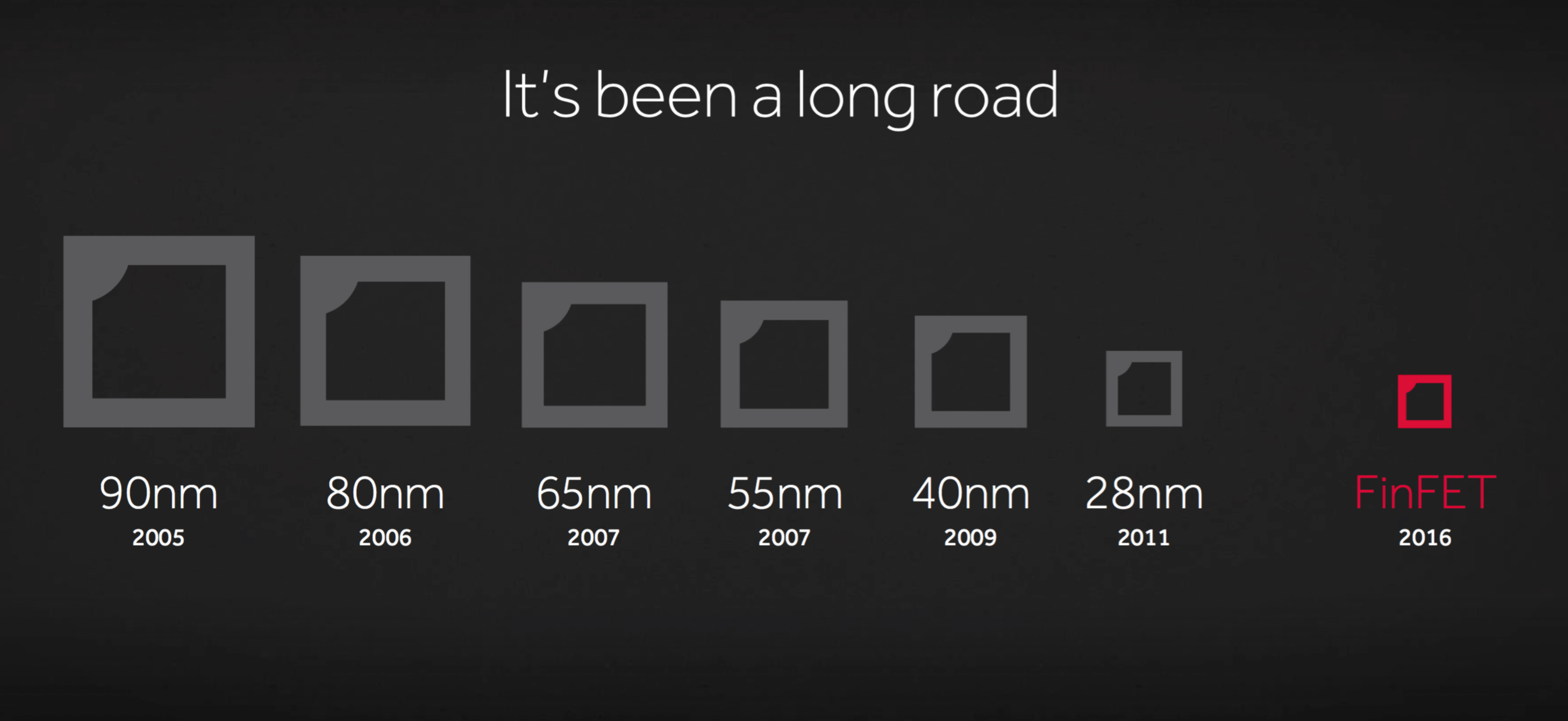
The main reason was the switch from using TSMC to GlobalFoundries for the manufacturing duties of the GPU. GloFo, as it's often called, formed in 2009 when AMD sold off its fabrication division, and for the production of Polaris they licenced Samsung's 14LPP process node.
This system used FinFETs instead of planar transistors, as used by TSMC in their 28HP node that made Polaris' predecessors. The update allowed for higher clock speeds to be achieved, while reducing power consumption at the same time, and offered much higher component densities.
The Radeon RX 480 wasn't designed to be the highest performing card on the market, just the most cost-effective one, and at $240 it appeared to fit that criteria on paper. In reality, it was no better than the likes of the older Radeon R9 390 and GeForce GTX 970, and despite both those models launching at almost $100 more, by this time they could purchased for the same price.
For AMD, though, tiny size meant production yields would be far better than those achieved with Fiji – better yields equals better profit margins.
Nvidia's Pascal architecture was hugely successful
Nvidia remained with TSMC, using their new FinFET 16FF node for the manufacturing of their new architecture, Pascal. This first came to market in May 2016, in the form of the GeForce GTX 1080.
Nvidia's design also reaped the benefits of the new transistor technology, and while not as small as Polaris 10, the GP104 chip that powered the 1080 was 21% smaller than the GPU in the GTX 980.
Packed inside the GTX 1080 were 38% more transistors (7.2 billion in total), clocked 42% higher, while consuming just 10% more power than its predecessor. It also sported a faster version of RAM, GDDR5X, giving it over 40% more memory bandwidth than the 980's GDDR5.
The MSRP was a steep $699, for the so-called 'Founders Edition' model, though third party variants started at $100 less. But coming in at around 60% faster, on average, than the GTX 980, and around 30% faster than AMD's best (the Radeon R9 Fury X), the performance improvement ensured it sold very well.
The GeForce GTX 1050 – compact and cost-effective
Over the next six months, Nvidia would go on to release three new GPUs using the Pascal architecture: the GP102, 104, and 106. The latter two would power the likes of the GTX 1070, 1060, and 1050 – all well received and popular purchases. The former would be used in Nvidia's most expensive single GPU desktop graphics card of its day.
The Titan X was launched with an asking price of $1,199 – 70+% more expensive than the GTX 1080. That enormous figure was matched by the GPU's specifications: 3584 shader units giving up to 11 TFLOPS of FP32 throughput, 12 GB of GDDR5X RAM, and 384 GB/s of memory bandwidth.
But for all that power, it wasn't 70% faster than the GTX 1080; many tests showed it to be around 25% better on average. Not that it seemed to matter, as the Titan X sold just as well as its lesser siblings.
The graphics card market of 2016 offered something for almost every budget, from $100 through to $1,000. GPU performance and stability was notably better than it had ever been before, and game developers started to take full advantage of their capabilities.
Nvidia was generating a healthy revenue and while its market share decreased due to the popularity of AMD's RX 400 product line, overall shipments of discrete graphics cards were steadily dropping, due to the long running decline in global desktop PC sales.
More cores, more heat... and more dollars
By now, GPU vendors had fallen into a reasonably predictable pattern: a new architecture would be released every two years or so, with lineup refreshes occurring in between, or sometimes both at the same time.
For AMD in 2017, it was a case of the latter. The Radeon RX 480 was given a minor clock bump and rebadged as the RX 580 – priced to undercut the GeForce GTX 1060 by $70, it performed a little faster overall, albeit with a higher power consumption.
GeForce GTX 1060 (left) and Radeon RX 580 (right)
The mid-range Radeon RX 560 was a notable improvement over the RX 460 it was based on: two extra Compute Units, more RAM, and higher clocks for a measly $99. Nvidia's GeForce GTX 1050, by now a year old, was slightly more power efficient and better performing, although the price tag was a little higher.
It's worth noting that the GP107 powering the 1050 was manufactured by Samsung, using their 14nm node – the same as that used by GloFo to make the Polaris 21 GPU in the RX 560. Both had a TDP (thermal design power) rating of 75W, despite the Nvidia processor having more transistors and higher clock speeds.
AMD's relatively weaker control over power was highlighted again with Radeon RX Vega cards, launched in mid-August. The Graphics Core Next architecture was refreshed once more, to version 5.0, and the GPUs were essentially Fiji reborn. The top-end RX Vega 64 sported a 12.5 billion transistor chip, 40% more than Fiji, but due to the better process node, it came in at 495 mm2 to the latter's 596 mm2.
Two 4 GB HBM2 chips sit next to a Vega GPU
The smaller chip also supported more RAM, thanks to using new HBM2 technology, and the overall performance was roughly the same as the GeForce GTX 1080. Despite its high power requirements (nearly 300W for some models), the standard version launched at $499 – a full $100 less than the 1080.
Not that Nvidia were particularly bothered. Their Pascal range of graphics cards were selling well, and in March they reinforced their hold over the enthusiast sector with the GeForce GTX 1080 Ti. This new graphics card used the same chip as found in the Titan X, albeit with fewer shader units enabled.
But with higher clocks, it performed virtually the same as the halo model but sold for $500 less which seemed like an expensive bargain in comparison. The launch also saw the MSRP for the GTX 1080 drop by $100, and sales of both models set new records for the Santa Clara firm.
Nvidia's GP102 GPU in the GeForce GTX 1080 Ti
Nvidia introduced a new architecture in 2017, but not for the general consumer. Volta was aimed at the professional compute market, but its design and feature set would come to strongly influence the direction of future GeForce products.
It was the first Nvidia chip to feature an exclusive architecture for a specific market. All previous compute-focused products, such as the Tesla K80, were derived from structures found in consumer desktop and mobile chips. Volta wasn't entirely different to Pascal, but at 815 mm2 in size, with 21.1 billion transistors and 5120 shader units, it was the largest processor they'd ever turned out.
At the other end of the scale, GPUs integrated into CPUs or system-on-chips (SoCs) had made solid progress too. Although Intel wasn't breaking any new technology boundaries with their Coffee Lake CPUs, their graphics architecture had reached Gen 9.5 and, depending on the CPU model, up to 48 EUs – each one now 7 threads wide, with up to 4 instructions co-issued per clock.
Naturally, gaming performance was still hampered by the overall scale of the GPU, and faired rather poorly against AMD's new Zen-based CPUs with integrated Vega GPUs. But it showed that Intel was still determined to improve the architecture.
This became particularly clear when they announced that AMD's head of the Radeon Group, Raja Koduri, had joined Intel with the specific goal of developing new discrete graphics products.
The last time Intel had offered a discrete graphics for the desktop PC market was nearly two decades ago, and while integrated GPUs was one thing, it was entirely different matter to scale such designs into competitive products to fight AMD and Nvidia's offerings.
The world of smartphones also saw consistent progress with their graphics processors. Apple was successfully using their own design, and although elements of the system used licenced technology from PowerVR, they announced that they would be parting ways – a move that did irreparable damage to the fabless company.
For Android fans, Arm offered the likes of the Mali-T860 and Qualcomm had a perfectly respectable GPU in their Snapdragon 600 series of mobile SoCs. Even Nvidia's two-year-old Tegra X1 chip found a popular home in the Nintendo Switch.
This should have been another 'golden year' for GPUs. There were numerous models for every budget and sector, and AMD and Nvidia seemed reasonably well matched except at the very top of the graphics performance ladder.
However, something that had been brewing in the background, for a number of years, suddenly exploded and PC gamers and enthusiasts bore the brunt of the aftershock. The use of GPUs for cryptocurrency mining dramatically rose due to the meteoric rise in the price of Bitcoin.
Supply of new GPUs ran dry and prices of second hand cards notably increased. GPU mining became a thing because the graphics processors were found to be extremely good at doing lots of simple mathematics en masse. AMD's GPUs were especially good at compute, although Nvidia's were more power efficient.
Regardless of the difference, both mid-range and top-end models saw consistent increases in price (as well as a continued dearth in availability), that ran well into the following year. And if consumers were hoping that the products for 2018 would be bring some sanity back to their wallets, they were in for a bit of a shock.
New technology, new marketing names, new prices
AMD enjoyed a successful launch of their fully redesigned Zen CPU architecture, after which it took a cautious approach to spend limited resources (both financial and physical) on developing their GPUs. Rather than refreshing a chip's internal features or introducing an update to Vega, they stuck to familiar grounds: rebadging.
Thus, the Radeon RX 500 series remained as it was from the previous year, albeit with an 'X' tacked onto the model name – for example, the RX 580 became the RX 580X, and so on. Some of the mid-range and budget models were given a boost to the amount of RAM they sported, but other changes were scarce.
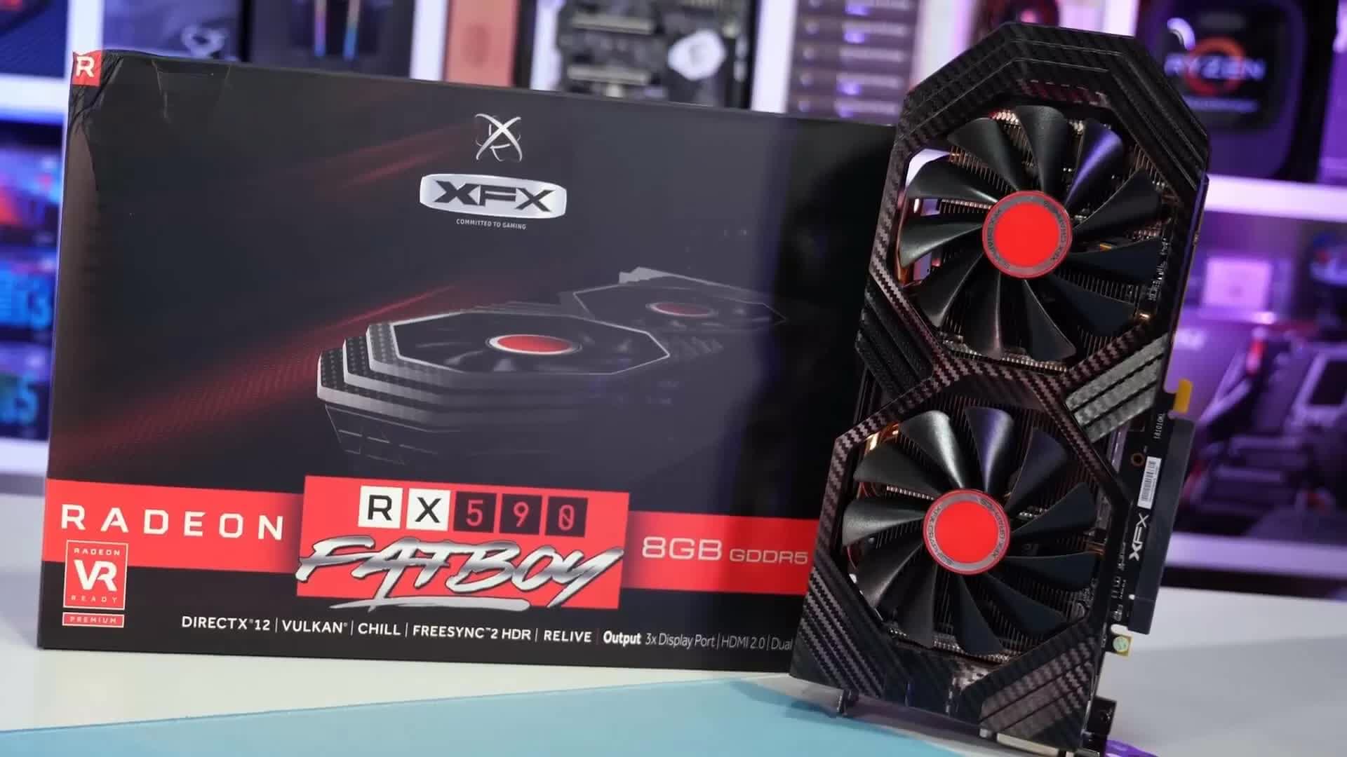
The only new product AMD brought to market was the Radeon RX 590. It used the same GCN 4.0 Polaris chip as the RX 580 and specs were almost the same, too. However, this chip was made by GlobalFoundries and Samsung, using improved process nodes (GloFo - 12LP, Samsung - 11 LPP).
The end result was a 5% reduction in the TDP, a 17% higher base clock, and a 15% higher boost clock – and an extra $50 on the MSRP, for good measure. Such minor changes didn't make the RX 590 stand out in any way, and the 580 (now in the form of the 580X) fared much better in stores.
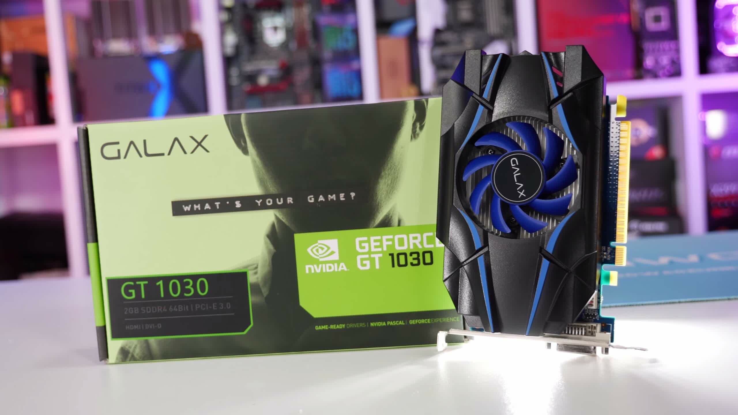
Nvidia started 2018 in a similar manner, bringing amended versions of their GTX 10 series to market, such as the miserable DDR4-equipped GeForce GT 1030. None brought anything new to the table, but it didn't matter so much in the first few months of the year, as GPU prices were so high.
By the summer, matters had improved, and PC enthusiasts eagerly awaited Nvidia's new architecture. The gap between new GeForce designs had been steadily increasing over the decade – 15 months separated Maxwell from Kepler, and there were 28 months between Pascal and Maxwell.
The first Turing GPUs appeared on shelves in August and September. The very first was a Quadro model for the professional workstation market. The GeForce lineup brought not just new GPUs and cards to buy, but new technology and marketing terms.
Nvidia had used the 'GTX' label as a prefix or suffix, since 2005 but now it was being replaced in favor of RTX, with the RT part effectively standing for ray tracing. Once the preserve of the film industry, the ability to more accurately model real-time lighting was becoming available in a standard desktop graphics card.
Earlier on Microsoft had announced a new API, called DirectX Raytracing (DXR) at that year's GDC event. They detailed how the system worked, and showcased a number of videos from EA, Epic, and Futuremark. While Nvidia and the RTX moniker were also involved, it was via Volta GPUs, not Turing.
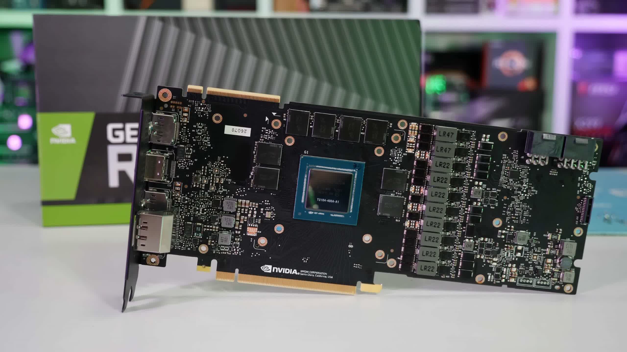
We got to see how this new architecture handled ray tracing with the GeForce RTX 2080 and 2080 Ti, both of which used the same TU102 chip. With 18.6 billion transistors and 754 mm2 in size, it made the Pascal-based GP102 look tiny in comparison. Despite sporting just over 4600 shader cores, it only had 20% more than its predecessor, so why was it so much larger?
The hulking TU102 processor – 60% larger than the GP102
Plenty of changes under the hood accounted for the increase. L1 and L2 caches doubled in size, the internal bandwidth greatly improved, and the addition of tensor and ray tracing cores to every SM (streaming multiprocessor) in the GPU all played their part.
The tensor cores – essentially a collection of FP16 ALUs, so they handled FP16 shader code, too – had surfaced in Volta, but had been updated slightly for Turing; the RT cores were completely new, with each one containing two specialized units: one for handling BVH traversal algorithms and the other for testing ray-primitive intersections.
Techno-babble aside, such circuitry isn't absolutely necessary, as ray tracing could be (and was) done on CPUs. But for doing it in real-time, in everyday games that anyone could buy, then such hardware was categorically required.
However, with no titles available for testing, offering DXR support or its equivalent via OpenGL/Vulkan extensions, when the new Turing chips appeared, reviewers turned to its raw performance in 'normal' games. The results, for the Ti version at least, were suitably impressive and further cemented Nvidia's hold over the top-end crown.
What was far less impressive, though, were the launch MSRPs – for the GeForce RTX 2080 Ti, Nvidia had set the tag at $999, and $699 for the 2080 (and $100 extra for Founders Editions).
In the case of the former, that was a full $300 more than the GTX 1080 Ti, although the RTX 2080 was a more palatable $100 increase over the 1080. But with GPU values only just returning to normal after the crypto mining debacle, a 43% increase in the price tag for the Ti was felt by many to be unjustified.
With the Turing line still being made by TSMC, albeit on a customized version of their 16FF process node (labelled 12FFN), the enormous chips would never generate the same level of yields that the 38% smaller Pascal GP102 dies could achieve. AMD had experienced a similar problem with the likes of Fiji and Vega, although they more willing to absorb the higher production costs.
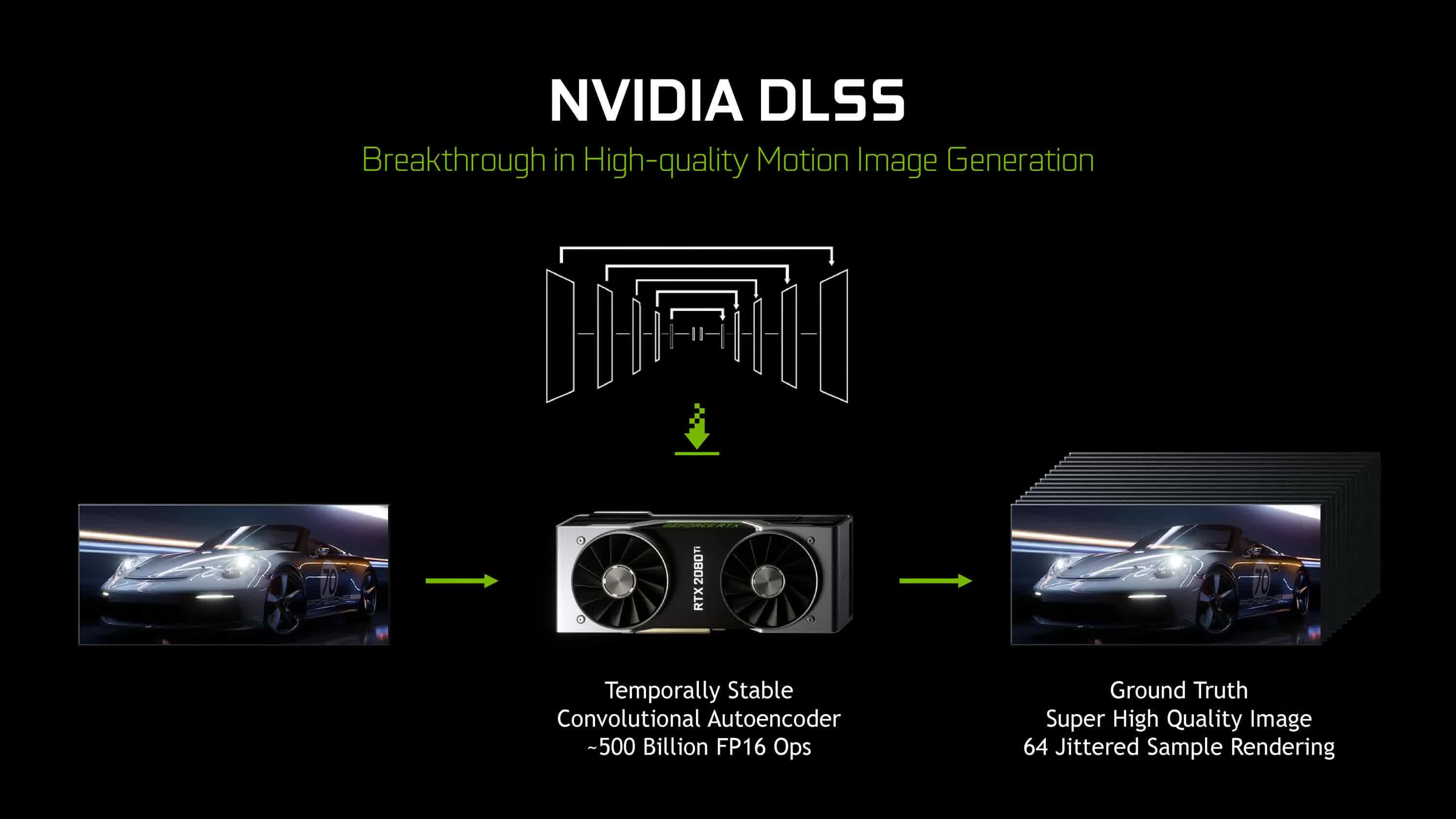
Another element of new GeForce RTX cards was much-touted by Nvidia: DLSS or Deep Learning Super Sampling. The general idea behind DLSS is to render everything at a lower resolution, then use an algorithm determined by machine learning to upscale the final frame to the monitor's resolution.
The tensor cores were promoted as being a key element behind this feature, but the first version of DLSS didn't use them in the consumer's graphics cards. Instead, this was all done by Nvidia's own computer grids, which were used to analyze each game, frame by frame, to work out what the upscaling routine would be.
Initial impressions were positive, as the lower resolution rendering improved performance, while the upscaling was good enough to maintain decent image quality. But as with ray tracing, there were no full games using the technology for the launch of Turing.
A swansong, a new start, and a change of heart
For hardware reviewers, the end of 2018 and the early months of 2019 gave them a better opportunity to examine Nvidia's RTX feature set. By then, there were several titles available that supported DXR and DLSS.
The likes of Battlefield V, Shadow of the Tomb Raider, and Metro Exodus all used the systems, to varying degrees, but two things rapidly became obvious: the use of ray tracing had the potential to significantly improve the realism of global lighting, shadows, and reflections. And second, the performance cost was exceptionally high, and only the use of DLSS helped maintain any semblance of playability. And this was at 1080p – resolutions higher than this were simply not an option.
While frame rates of 30 fps or below were often the norm for consoles, when running games with extreme graphics, it was the antithesis of what PC enthusiasts had come to expect when shelling out $1,000 for a graphics card.
Around this time, both AMD and Nvidia released new graphics cards – the former gave us the Radeon VII, whereas the latter offered the GeForce RTX 2060 and the return of the GTX moniker, with the 1660 Ti.
Saying goodbye to GCN with the Vega 20 chip
The Radeon VII would be GCN's swansong: the last version of that long-running architecture, or so it would seem, before AMD switched to something new. The chip powering the card was the Vega 20, a version of that found in the Radeon Vega 64, albeit with a few tweaks, and manufactured on TSMC's new 7N node.
On paper, the model had everything going for it: 16 GB of HBM2, sporting 1024 GB/s of bandwidth, along with 60 Compute Units running at up to 1,800 MHz.
With an asking price of $700, AMD was pitching it against Nvidia's GeForce RTX 2080 and on average, it was only a few percent slower in testing. But the product was never intended for gamers, as it was just a rebadged Radeon Instinct, a workstation-level compute model.
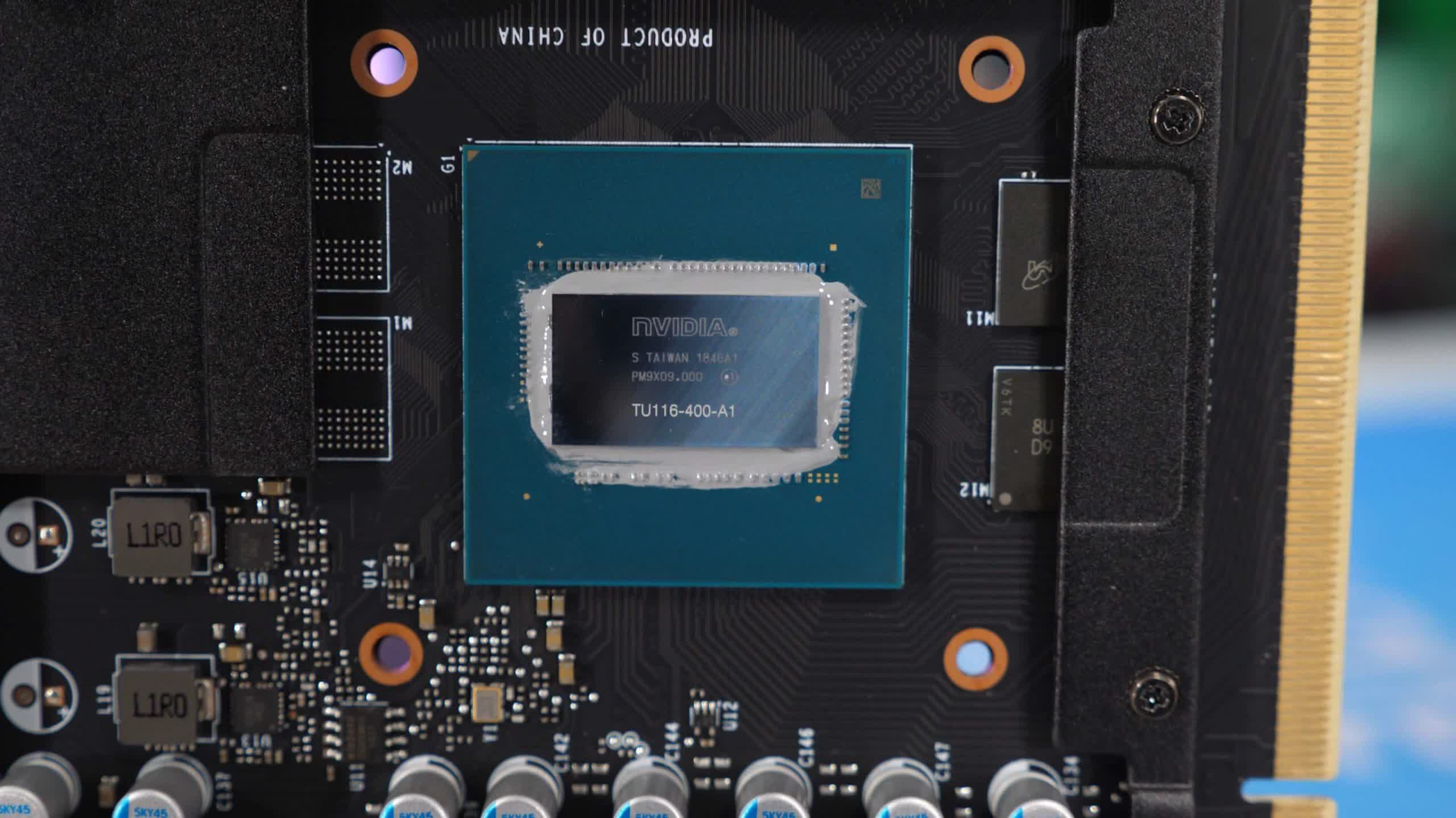
The TU116-powered GeForce GTX 1660 Ti, on the other hand, was absolutely targeted at gaming – especially for those with a clear mind on budget. For $279, you could say goodbye to Tensor and RT Cores and hello to a product to that was on-par with the $100 more expensive Pascal GTX 1070.
No ray tracing or tensor cores for this Turing GPU
The GeForce RTX 2060 released at the start of 2019, retaining all RTX features, it was nearly 30% more expensive than the GTX 1660 Ti, but only 12% faster on average, so it didn't offer the same value for money.
Both mainstream models offered some relief against Nvidia's pricing of their enthusiast-level RTX models though – in the case of the 2080 Ti, it had risen by over $300. Later they would be joined by the likes of the GTX 1650, released at $149.
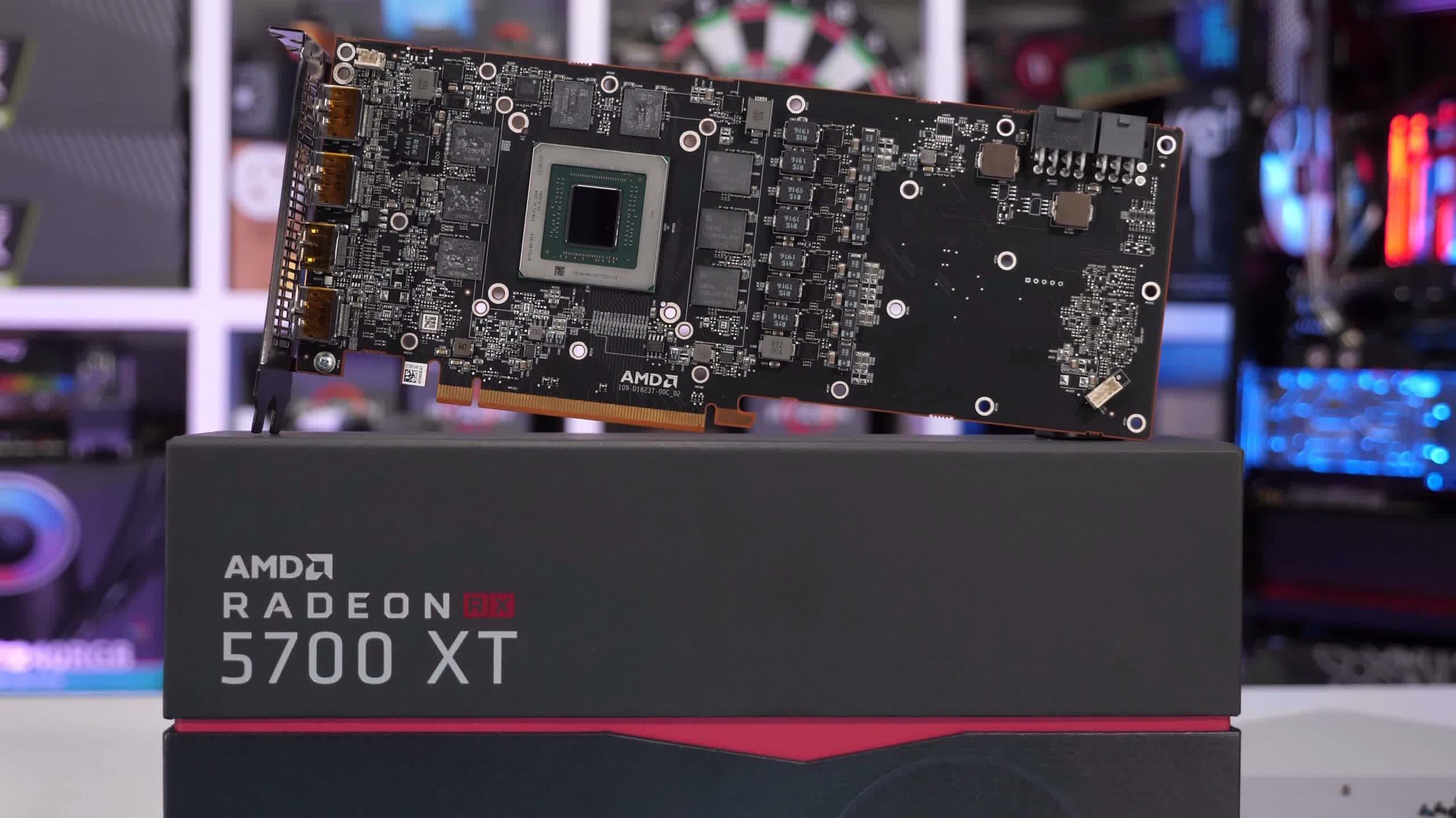
AMD held their new architecture hidden away until the summer, when they released the Radeon RX 5000 series, powered by Navi 10 chips. The GCN architecture had been given a thorough overhaul, transforming into RDNA, and with it addressing many of the limitations that the older design suffered from.
Goodbye GCN and hello to the start of a new architecture
Where Nvidia was aiming to please all markets with Turing, casual and professionals alike, RNDA was all about games. The basic specs pointed to it being worse than the Radeon Vega 64, with significantly fewer Compute Units. But AMD reworked the architecture to improve instruction issuing and internal data flow, and the end result was a graphics card that wasn't that far behind a Radeon VII and GeForce RTX 2070. Launching at $399, it undercut both models, and with the chip being a svelte 251 mm2 in size (due to TSMC's 7N node), it gave AMD good yields too.
While some people were disappointed that the new GPU wasn't a top-end model, and criticisms over stability and drivers would eventually become newsworthy, Navi proved that it was possible to have decent gaming performance without the need for enormous chips and price tags.
Nvidia had readied a response to the Radeon RX 5000 family in the form of 'Super' models – over the course of 2019, the RTX 2080, 2070, 2060, GTX 1660, and 1650 would all be refreshed with GPUs sporting more shader cores and higher clock speeds. The extra performance was welcome as was the fact that the MSRPs hadn't changed, bar the 2060's.
Intel's discrete GPU project was starting to take shape. By now it had a clear name, Xe, and some details about potential models were being discovered. Its first outing though, would still be in the integrated graphics market.
An end of a decade – new chips, new threats, worse problems
2020 would turn out to be a year of disparate fortunes. Against the background of a global pandemic, AMD, Intel, and Nvidia all released new graphics cards containing new architectures and product designs.
Microsoft and Sony also brought fresh consoles to market, sporting a raft of new technologies and features, with the former consolidating several years of API updates with the release of DirectX Ultimate.
Hidden by the heatspreader, Nvidia's largest ever GPU: the GA100
The professional world of compute and AI were given the likes of the AMD Radeon Instinct MI100 and Nvidia A100, both featuring gargantuan GPUs (750 and 856 mm2 respectively) with enormous power (120 CUs giving 23 FP32 TFLOPs or 432 Tensor Cores producing 312 BF16 TFLOPs).
The former fielded AMD's new CDNA architecture, GCN reborn into a compute-only market, whereas Nvidia used the new Ampere design. It was marketed as a direct replacement for Volta, offering large performance increases for AI workloads.
Speaking of AI, Nvidia introduced an improved version of DLSS in March, which used a very different process to the first iteration. Now, the tensor cores in users' graphics cards would process the inference algorithm to upscale the image, and overall, the new system was well received.
Desktop PC enthusiasts would have to wait to later in the year for a new batch of GPUs, but their patience was rewarded by the GeForce RTX 3000 and Radeon RX 6000 series of cards. Nvidia's models brought Ampere to the masses, although there were significant differences between the GA100 chip in the A100 and the GA102 that drove the RTX line-up. The latter was essentially an update of Turing, featuring improvements to the CUDA, Tensor, and RT cores.
Nvidia's unusual design for the cooling system in the GeForce RTX 3080
In the case of the general shader units, the integer ALUs could now handle the same FP32 routines as the FP ones, and Nvidia utilized this to promote the 3000 series having double the number of cores as their predecessors. While not entirely true, it did mean that the GA102 had the potential to offer substantial floating point throughput.
But as games are not entirely limited by their FP32 shaders, the overall performance of the RTX 3090, 3080, and 3070 was less than the paper specifications suggested, though still a sizeable improvement over Turing. Better yet, launch prices were generally lower than those for the RTX 2000 range.
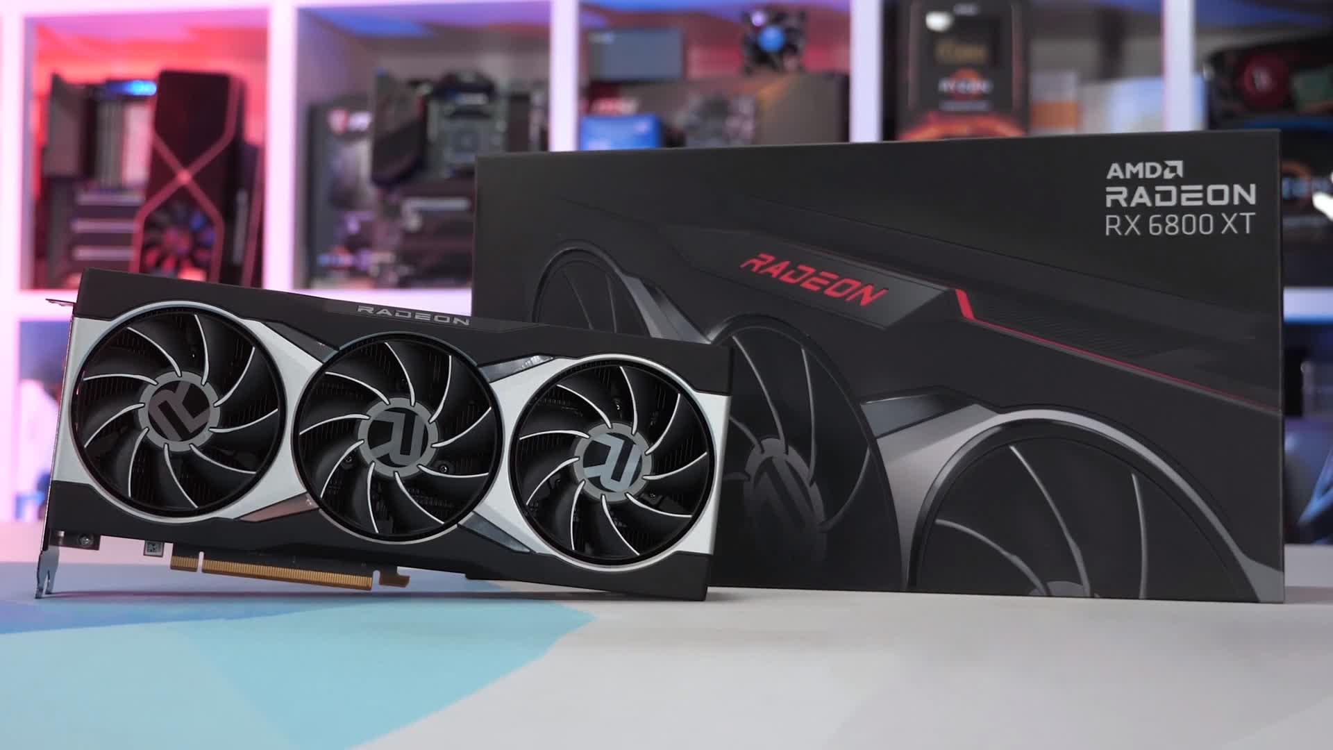
AMD took RDNA and tweaked critical aspects of it, such as power consumption, operating frequencies, and data throughput, to mitigate the factors that ultimately limited the capabilities of the RX 5000 cards. RDNA 2 showed that the consistent progress made with the Zen architecture was going to a company-wide goal.
Popularly known as 'Big Navi', the Navi 21 GPU housed twice the number of Compute Units than its predecessor, a substantial 128 MB of L3 cache, and adapted texture processors that would handle the ray-triangle intersection checks in ray tracing.
The Radeon RX 6000 series would put AMD on a level playing field with Nvidia in most games, although the cards were notably worse when ray tracing was involved, and offered nothing like DLSS to boost performance.
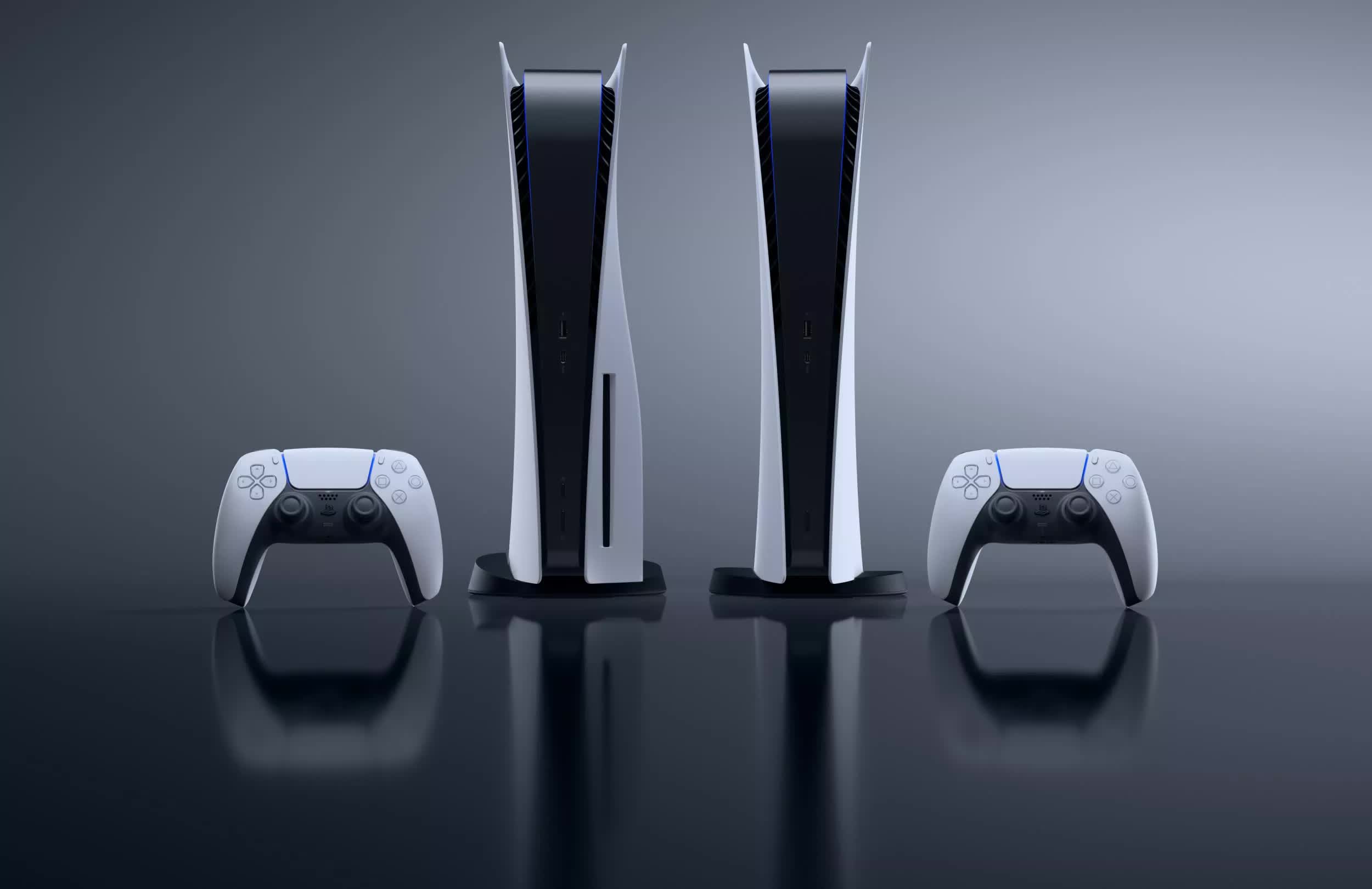
The same RDNA 2 architecture, albeit with far fewer CUs and no extra cache, would power the new Xbox and PlayStation consoles. Coupled with Zen 2 processors on the same die, the updated systems left gamers salivating at the potential the devices had to offer.
Even Intel finally released a new discrete GPU, though only to OEM and system builders. Previously known as DG1, the Iris Xe desktop card was nothing to get excited about, but it highlighted that Intel were serious about competing in the graphics market.
All of the excitement and enthusiasm about the new releases would eventually turn to frustration and anger, as the usual problems of supply and exaggerated prices grew to farcical proportions. For desktop Ampere, Nvidia chose to use Samsung for fabrication duties and while never directly confirmed, the general impression, felt by many industry, was that their yields simply weren't as good as TSMCs.
Not that it ultimately mattered. As 2020 drew to a close and the new decade started in earnest, the demand for electronics and computing devices skyrocketed, due to millions of people around the world being forced to work from home. As the effects of Covid grew more serious, the production of basic components, such as voltage regulators and microcontrollers, became increasingly limited.
Supplies of GeForce and Radeon graphics cards turned exceptionally sparse, a matter not helped by another burst in crypto mining and the pervasive use of bots to mass purchase cards and consoles from websites. Almost every available GPU model significantly rose in price and second hand prices matched or exceeded their original launch values.
And where the general consumer struggled with the dearth of options, AMD and Nvidia both enjoyed significant increases in the revenues, with the latter experiencing nearly a 30% growth in their gaming sector. Such figures would offer scant comfort for PC gaming enthusiasts, many of which were unable or unwilling to pay the extortionate prices that graphics cards were now demanding.
What does the future hold?
As we conclude the fifth part of our series on the history of the modern graphics processor, it would be remiss not to look ahead and speculate about what the next decade might hold. The challenges related to supply and pricing are not permanent, but there are no immediate signs of improvement.
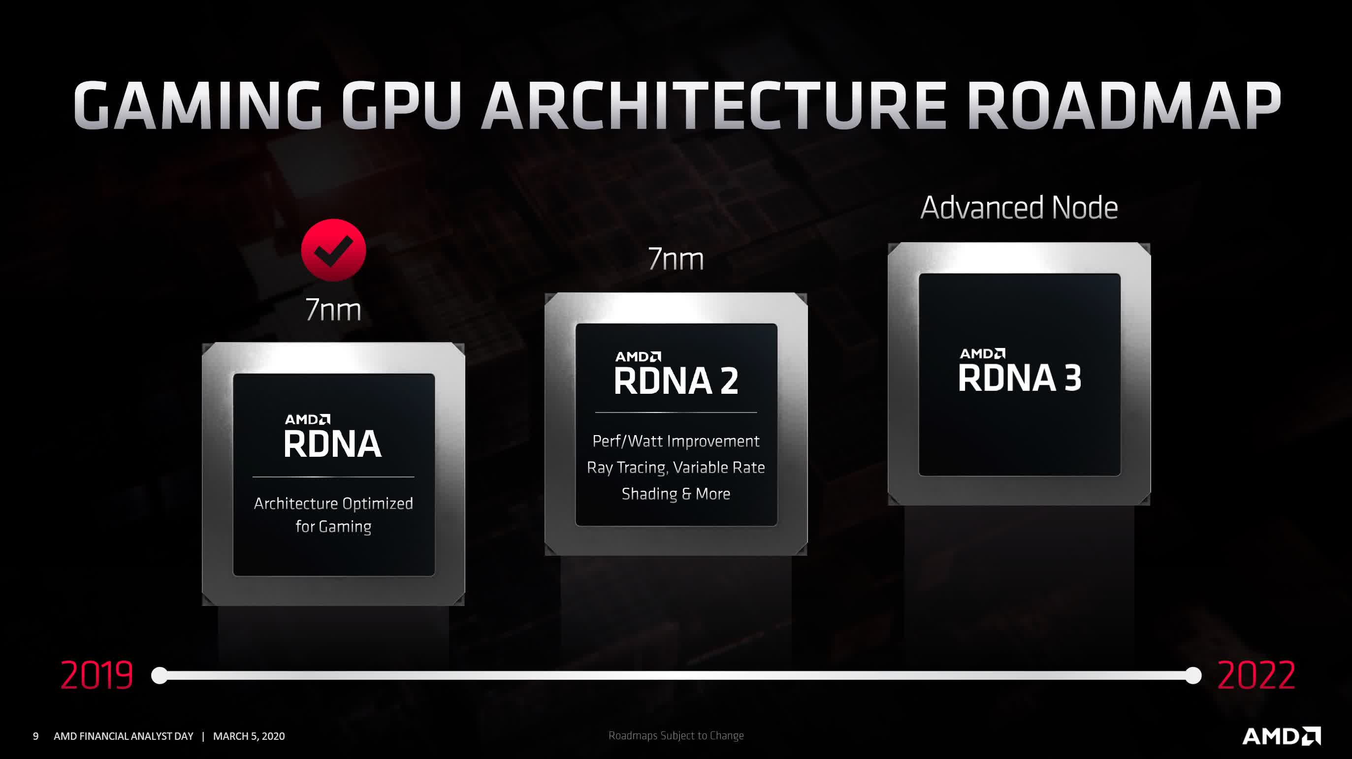
We do know that AMD had targeted 2022 for releasing updates to their gaming and compute architectures: RDNA 3 and CDNA 2. Whether this timeline will hold true, given various external circumstances, is difficult to predict. However, it's unlikely that these developments will be delayed much beyond that timeframe.
Fundamentally, RDNA 2 is a refined version of its forebearer, with performance gains coming from a mixture of design changes to improve clock speeds, pipeline efficiency, and reduced data movement. The only new feature are ray accelerator units, integrated into the texture processors.
We certainly won't see a new major version of DirectX in 2022, so RDNA 3 is likely to be more of the same optimizations and tweaks. The above image states that it will also be manufactured on an 'Advanced Node' but this tells us very little. Will they use TSMC's EUV-based N7+ node, or another one, such as N6 or N5?
The Navi 21 GPU used for the Radeon RX 6800 series is one of AMD's largest chips ever designed for the desktop PC market, at 520 mm2 (only Fiji was larger). But as this is still 30% smaller than Nvidia's TU102, it would suggest that there's scope for an even larger processor to hit shelves.
Will the next decade of GPUs be just updated versions of RDNA 2 and Ampere, or is something entirely new on its way?
Nvidia is considerably more reticent to publicly issue roadmaps, and little is known about what's next for them, other than rumors of it being called Hopper (named after Grace Hopper, a pioneer in computer science). Like RDNA 2, Ampere was an optimization of Turing, and having settled on a GPU structure that's changed relatively little over the year, there's a strong chance that it will be more of the same.
And like AMD's Navi design, there's scope for the next round of Nvidia GPUs to sport even more shader units, cache, and so on – even if they retain Samsung for manufacturing duties, and don't even alter the node, the likes of the GA102 can be made 20% larger before it hits the same size as the largest Turing processor.
If we ignore GPUs like Volta, which weren't intended for the consumer market, the TU102 was the largest single GPU to be manufactured and sold for desktop PCs. At 754 mm2, it greatly restricted the number of dies that could be extracted from a single 300 mm wafer – around 80 or so, at best. So could we see chips that size again?
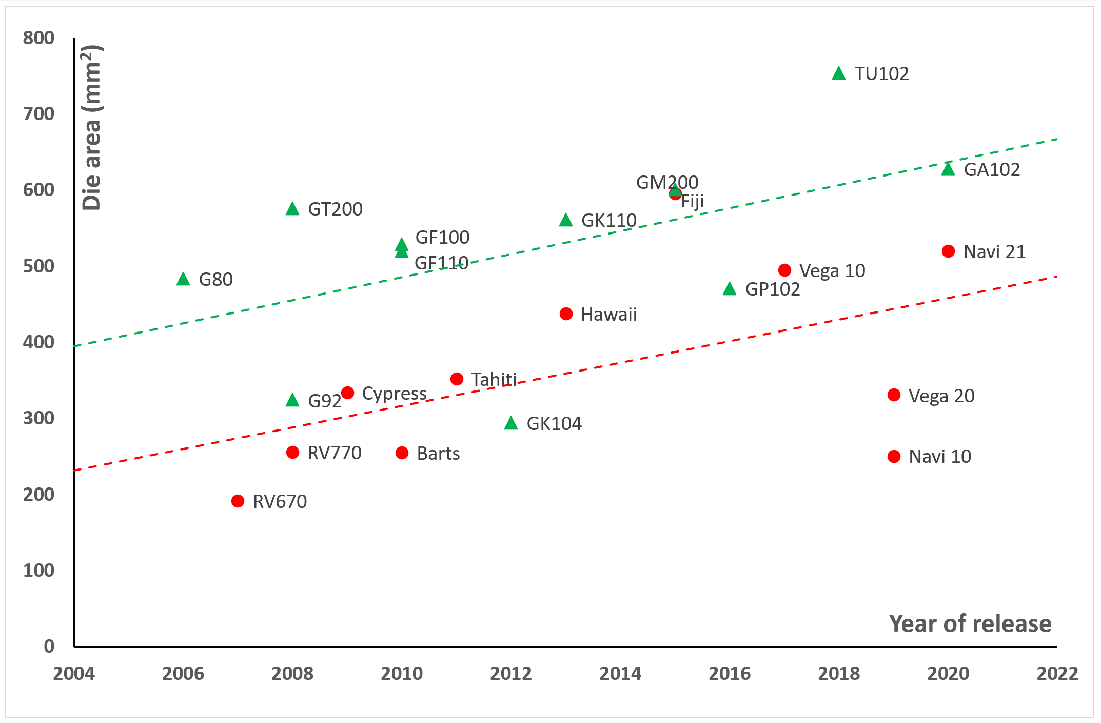
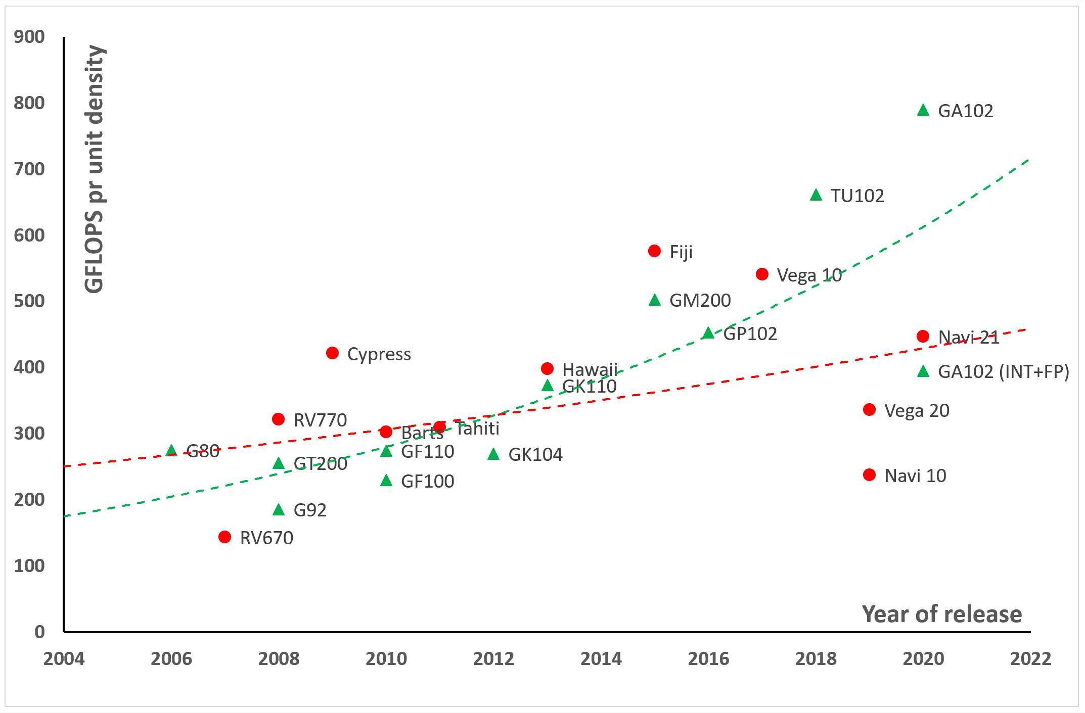
Taking a sample of AMD and Nvidia's largest GPUs over the years shows a vaguely linear trend in the growth of die sizes, but it also highlights how altering the process node can make an enormous difference (for example, compare Vega 10 and 20 sizes). However, there's far too much variation in the data for it to be used to reliably estimate what size of processor one could be seeing over the next ten years.
Perhaps a better approach would be to look at the processing power the above GPUs offered, for the given unit density (i.e. millions of transistors per square millimetre). While peak FP32 throughput, measured in billions of floating point operations per second, isn't the only metric that should be used to judge the capability of a GPU, it is a comparable one. This is because general shader operations form the bulk of the processing load and will continue to do so for a while.
When we look at a graph of those figures (below), it paints a rather different picture. There are outliers that affect the trends somewhat, but even with them removed, the overall pattern is broadly the same.
It shows us that Nvidia has consistently focused on increasing raw processing power with each new design – something that makes sense given how the same chips are used in general and professional models. The same was true of AMD until they released RDNA, where the product is solely aimed at gaming.
GCN lives on in the form of CDNA and also in integrated GPUs in Ryzen APUs, and although there is only one GPU using that architecture, it would actually place lower than Navi 21 does on the chart. This is because that design is targeted for AI workloads, where standard FP32 processing is less important than integer and tensor workloads.
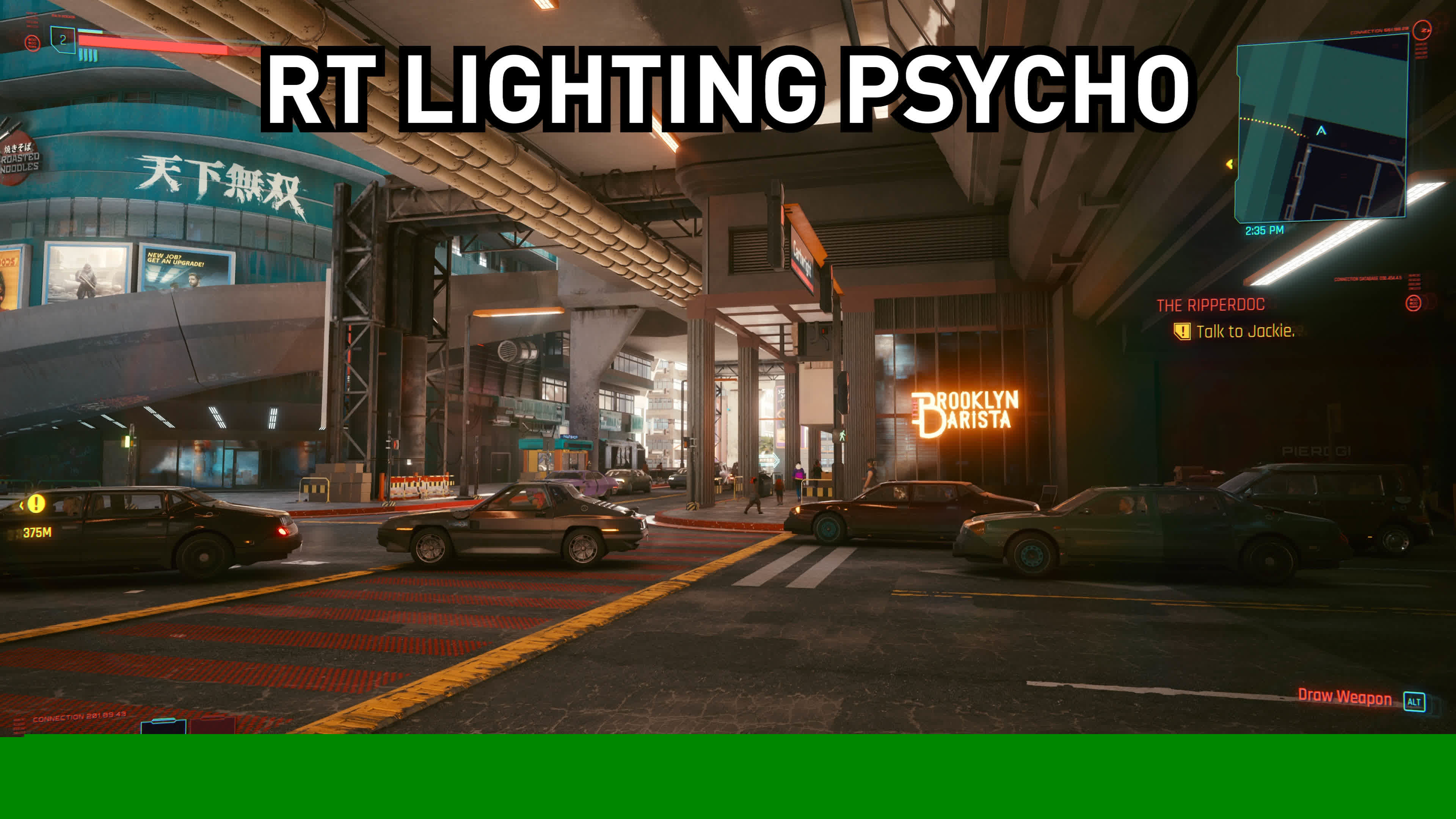
With both Nvidia and AMD offering ray tracing acceleration, as well as support for data formats and math operations needed for machine learning in their latest GPUs, PC and console games of this decade are increasingly going to utilize them. Just as anti-aliasing and tessellation were once too demanding and could only be used sparingly, the same will be true of today's performance hogs.
It won't take to 2077 for games to routinely be using psycho levels of ray traced global lighting
Does this mean that GPUs of 2030 will be routinely hitting 800 mm2 in size and produce well over 1 TFLOP per unit density? Will they increasingly favor ray tracing and machine learning over traditional aspects such as general purpose shaders or texture processing?
Possibly, but there's a critical aspect to all of this that may curtail such growth patterns or changes in fundamental GPU design, and it all revolves around data movement.
Having thousands of shader units, tensor or ray tracing cores is all well and good, but they'd be left hung out to dry if they couldn't fetch or write data fast enough. This is why cache size and internal bandwidth has grown so much, ever since the start of the GPGPU industry.
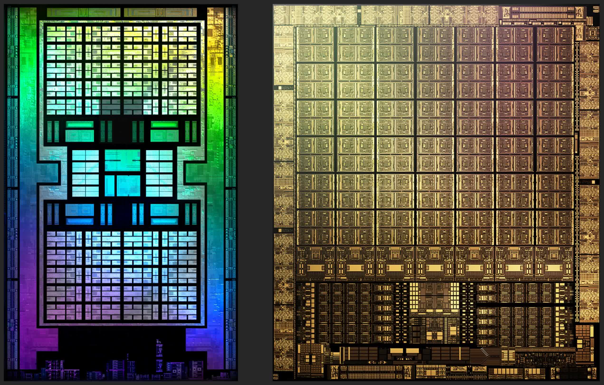
The G80's SMs are the pink/green pair of blocks at top and bottom. Between them lies the texture units and cache. Image: Fritzchens Fritz
The Nvidia G80, the company's first chip to use unified shaders, sported just 16 kB of shared memory for each SM (streaming multiprocessor), 16 kB of texture cache for a pair of SMs, and a total of 96 kB of Level 2. Compare that to the GA102, where each SM gets 128 kB of L1 cache and the whole GPU contains 6144 kB of L2.
As process nodes develop and component features reduce in size, it would seem that even more can be packed in. However, SRAM (the primary building block of cache) scales down far worse than logic systems do, and with so much of a modern graphics processor being cache, chip sizes may well balloon in size without increasing the shader count or ray tracing ability by the same scale.
Or it could well be the other way round. Nvidia (and others) have done significant research into scaling GPU performance by using a modular design – i.e. having multiple smaller dies on the same package, much like AMD does with chiplets on Zen-based CPUs.
GPUs in the desktop PCs of 2030 won't be this big!
While such research was predominantly for the professional market, it's worth remembering that many of Volta's features found their way into Turing, so it could be possible that gamers at the end of this decade will have PCs sporting numerous CPU and GPU chips, all packed into relatively compact packages.
But regardless of what format they take, tomorrow's GPUs will continue to push the boundaries of VLSI chip design and microprocessor fabrication. The raw capabilities of future GPUs in terms of FP32 throughput and internal bandwidth will reach levels that could only be dreamed about, just 10 years ago.
And with Intel and others determined to force their way into the market, to capitalize on the growth of GPGPU in AI, we can be certain of one thing: AMD, Nvidia, et al are all still many years away from reaching the limits of what they can achieve with their graphics processors.
TechSpot's History of the GPU
The modern graphics processor has become one of the largest, most complex, and most expensive components found in almost any computing device. From the early VGA days to the modern GPU. The history and evolution of the chip that came to dominate gaming, and later AI and compute.