AMD Ryzen 9 7940HS APU with Radeon 780M iGPU shows stunning gaming performance

DragonSlayer101

Posts: 371   +2
Staff
What just happened? Benchmark results published by popular YouTube channel ETA Prime show that AMD's Ryzen 9 7940HS mobile APU can offer smooth 1080p gameplay in a slew of well-known games, including Counter-Strike: Global Offensive, GTA 5, Forza Horizon 5, Fortnite, Doom Eternal, and more. The testbed was the 2023 ASUS TUF A15 laptop, which comes with 32 GB of DDR5-5200 RAM overclocked to 5600MHz. It also had an RTX 4060 discrete graphics card, but it was disabled for the purpose of these tests.

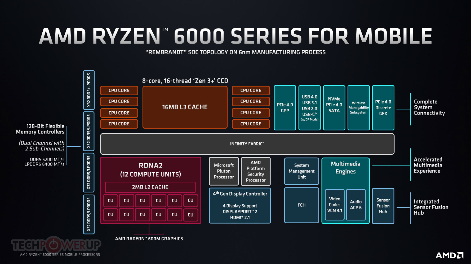
The Ryzen 9 7940HS is the flagship SKU in AMD's Ryzen 7040 lineup. It comes with the RDNA 3-based Radeon 780M iGPU with 12 Compute Units, clocked at up to 2.8GHz. On the CPU side, it has 8 Zen 4 CPU cores, 16 threads, a 4GHz base clock, 5.2GHz boost clock, and 40MB of total cache. A stress test on Furmark showed that the 780M drew around 45W of power.

Coming to the benchmarks, the CPU (limited to 80W) racked up 11,453 points in 3DMark Time Spy, while the GPU scored 2,830. That's slightly higher than the 2,400 points notched up by the Radeon 680M, but a tad less than the 3,200 points scored by the Nvidia RTX 2050 mobile GPU. It also surpassed the Radeon 680M handsomely in 3DMark Fire Strike.

Getting to the gaming benchmarks, CS:GO running at 1080p High achieved a smooth 138 FPS average, and even hit 150+ occasionally. GTA 5 and Forza Horizon 5 with the same settings achieved an average of 81 and 86 FPS, respectively. As for Fortnite and Doom Eternal, they hit an average of 78 and 83 FPS, respectively, at 1080p Medium.

The video also revealed benchmark results for Horizon Zero Dawn, Call of Duty: Modern Warfare II, and Cyberpunk 2077. Starting with HZD, the 7040HS got an average of 69 FPS (1080p Favor Performance), while COD: MW II hit an average of 106 FPS at 1080p using the FSR 'Performance' mode. Finally, Cyberpunk 2077 ran at around 77 FPS at 1080p with a mix of low and medium settings.

The Asus TUF A15 laptop is expected to be one of the many notebooks to be launched with AMD's new Ryzen Mobile 7040 series CPUs. According to a recent report, the first set of laptops featuring the Ryzen 9 7840HS will hit retail shelves in North America in late April, while those with the 7840U is tipped to debut in early May.

Permalink to story.

 
Now imagine an APU with 3Dv cache...
Probably wouldn't help that much because even with the 780M, the majority of games are still going to be GPU-bound and the graphics core of the APU has no access to the CPU's cache structure.
 
Probably wouldn't help that much because even with the 780M, the majority of games are still going to be GPU-bound and the graphics core of the APU has no access to the CPU's cache structure.
Imagine stacked cache that the iGPU could access. Maybe a separate cache, maybe AMD resurrects hsa, or most likely the cache is designated for CPU or GPU use with a bios option.
 
While iGPU are capable of running last year's games at reasonable frames now, it will become a stuttering mess with some of this year's titles, and it will continue to get worst.
 
Probably wouldn't help that much because even with the 780M, the majority of games are still going to be GPU-bound and the graphics core of the APU has no access to the CPU's cache structure.

yea you're right I know, I was more thinking about something like that ->

Imagine stacked cache that the iGPU could access. Maybe a separate cache, maybe AMD resurrects hsa, or most likely the cache is designated for CPU or GPU use with a bios option.
 
Imagine stacked cache that the iGPU could access. Maybe a separate cache, maybe AMD resurrects hsa, or most likely the cache is designated for CPU or GPU use with a bios option.
The problem is that the L3 cache in Zen CPUs is a victim cache -- it just stores data that's been evicted from L2. The cache requirements and usage in GPUs are somewhat different and making an L3 that suits all needs, for both CPU and GPU, would probably be deemed too costly.

It's been done before, of course -- Intel used an L4 cache in some of its older CPUs used on-die SRAM to store L4 cache tags and a separate eDRAM die for the actual cache. It was designed for use by both the CPU and integrated GPU, but the latencies were pretty poor. Modern foundry nodes could get this all one-die, as SRAM (just like the L3 cache in Navi GPUs), but it would make the whole die (Phoenix is monolithic) quite a bit larger and more expensive to produce.

The reality is that there are just not enough Compute Units in an integrated mobile GPU to warrant the addition of an L3 cache.
 
Technically, wouldn't this be more powerful than the GPU in the XSS?
780M 12CUs = 768 shaders (768*2*3.0)/1000 = 4.6TFlops
XSS 20CUs = 1280 shaders (1280*2*1.56)/1000 = 4TFlops

That's about a 13% increase in FP32 performance.

I wonder if this would hold up in real world gaming?
 
Technically, wouldn't this be more powerful than the GPU in the XSS?
780M 12CUs = 768 shaders (768*2*3.0)/1000 = 4.6TFlops
XSS 20CUs = 1280 shaders (1280*2*1.56)/1000 = 4TFlops

That's about a 13% increase in FP32 performance.

I wonder if this would hold up in real world gaming?
Not seen any in-depth details pertaining to the 780M yet, but if it's a 'full' RDNA 3 design then each Compute Unit will have double the number of FP/INT ALUs per Stream Processor than in RDNA 2.

So the FP32 FMA rate would be:
Radeon 680M = 768 ALUs @ 2.2 GHz = 3.379 TFLOPS
Radeon 780M = 1536 ALUs @ 2.8 GHz = 8.602 TFLOPS
Xbox Series S = 1280 ALUs @ 1.575 GHz = 4.032 TFLOPS
Xbox Series X = 3328 ALUs @ 1.875 GHz = 12.48 TFLOPS

However, the shader compiler needs to work hard to ensure the ALU occupancy is kept really high, to take advantage of the double ALU setup.
 
but it would make the whole die (Phoenix is monolithic) quite a bit larger and more expensive to produce.
We're talking stacking of the extra cache, which likely is possible even with a monolithic die if they designed it that way. Might be even easier as there's potentially more "cold" silicon to put the cache on top of. It would be more expensive but if the product is that much better it'd be sold as more expensive.

One thing I find interesting are the Zen4C cores that are space-optimised for the latest servers to be able to cram more cores than Zen4. The main way they've done this is by cutting L3 cache. Once stacking becomes more mature this may be the way they go for normal parts, something like a small die with 16MiB cache which ships that way for the low end with a stack for the mid and maybe multiple stacks for the high end. When stacking becomes very mature they may decide to remove L3 from the main die altogether. I mention this as it could be how they keep monolithic die sizes in check.

The reality is that there are just not enough Compute Units in an integrated mobile GPU to warrant the addition of an L3 cache.
They've sized the iGPU to the constraints of the environment, a big one being memory bandwidth. Access to even a small L3 cache for the hottest of data should allow the iGPU to be usefully bigger.
 
We're talking stacking of the extra cache, which likely is possible even with a monolithic die if they designed it that way. Might be even easier as there's potentially more "cold" silicon to put the cache on top of. It would be more expensive but if the product is that much better it'd be sold as more expensive.
Zen L3, integrated or stacked, is still a victim cache -- for it to be a fully inclusive cache, accessible by both CPU and GPU, would require an overhaul of the cache system which would make the die larger. Even if one just made the stacked cache to be like this and left the CPU L3 as it is, (I.e. the V-cache is effectively a Level 4 cache), the overall die is still going to be larger.

They've sized the iGPU to the constraints of the environment, a big one being memory bandwidth. Access to even a small L3 cache for the hottest of data should allow the iGPU to be usefully bigger.
AMD's monolithic APUs are designed to have 'just enough' GPU performance -- for anything more than that, the expectation is that vendors will turn to its mobile GPUs, which do have L3 cache.
 
I have not seen a 7000 series mobile APU block diagram, but here is a 6000 series APU:

3SAD3GYc6USmgKT6.jpg
 
I have not seen a 7000 series mobile APU block diagram, but here is a 6000 series APU:
Comparing AMD's listed specifications for the 7940HS to those for the 6890HX, the block diagram is going to be very similar, if it ever gets released. The newer APU has far better RAM, USB, and PCIe support than the older one, but caches levels in the CPU are the same -- no word yet if the RDNA 3 GPU has the same characteristics as the desktop version, though.
 
AMD's monolithic APUs are designed to have 'just enough' GPU performance -- for anything more than that, the expectation is that vendors will turn to its mobile GPUs, which do have L3 cache.

I have the feeling that your statement could sadly be true. G series have been quite impressive for the price but the graphic part hasn't progressed much between 2200g and 5600g.
 
I have the feeling that your statement could sadly be true. G series have been quite impressive for the price but the graphic part hasn't progressed much between 2200g and 5600g.
Bcz AMD has a plan....

There is no sense doing a larger APU until you have more pins. You need more contacts to make a more graphically intense APU.

I think you'll be quite impressed with what AMD can do with AM5 socketed APU. If they can manage to stuff around 40 CUs (of RDNA3) on an APU... conservatively that would make low end discreet GPUs obsolete.

This 780m is impressive... I hope to find a 7940hs in a 13" notebook that sans a dGPU.
 
AMD's monolithic APUs are designed to have 'just enough' GPU performance -- for anything more than that, the expectation is that vendors will turn to its mobile GPUs, which do have L3 cache.
What "just enough" is is a matter of debate though. The 2 CU's on every 7000 series CPU is probably fine for a basic desktop experience, yet they've maxed out what the memory bandwidth can reasonably handle with a dozen CU's on APU's. If APU's can eat further into low end dGPU by adding L3 to combat bandwidth limitations, I don't see why they wouldn't. The chiplet design of dGPU's may not scale to the very low end without disabling half of a single die, which will rarely happen naturally but can be easily soaked up by a trash OEM card for a prebuilt.
 
If APU's can eat further into low end dGPU by adding L3 to combat bandwidth limitations, I don't see why they wouldn't.
AMD doesn't want its APUs to have a significant rendering uplift over its discrete Radeon chips, be them mobile versions or anything else. The Phoenix lineup isn't the cheapest thing to manufacture as it already is, being on TSMC's N4 node and having a die size of 176 mm2. That's barely any smaller than Cezanne.

The chiplet design of dGPU's may not scale to the very low end without disabling half of a single die, which will rarely happen naturally but can be easily soaked up by a trash OEM card for a prebuilt.
Low-end RDNA 3 GPUs will still be monolithic.
 
AMD doesn't want its APUs to have a significant rendering uplift over its discrete Radeon chips, be them mobile versions or anything else. The Phoenix lineup isn't the cheapest thing to manufacture as it already is, being on TSMC's N4 node and having a die size of 176 mm2. That's barely any smaller than Cezanne.

Dr Lisa Su's mission statement was that only high-end gamers and workstations will need supplemental GPUs and sees a heterogeneous solution as the answer for sharing resources on a die. It's on their roadmap, AMD is just waiting for the right time to use fabric, chiplets and "shared" L3 for the hat trick...

RDNA3.5 is coming soon for APUs... and yes we might see an APU that topples even the RTX4060/6600 at 1080p...

Anything under navi33 will be served by APU.
 
Back