Chip makers are slowing down on the way to 7nm

Greg S

Posts: 1,607   +442
Bottom line: Building even smaller transistors has gotten too expensive for the majority of design firms in the near term. Even though 7nm is now possible, only pricey chips with high performance or extraordinarily low power consumption will make use of the latest process node.

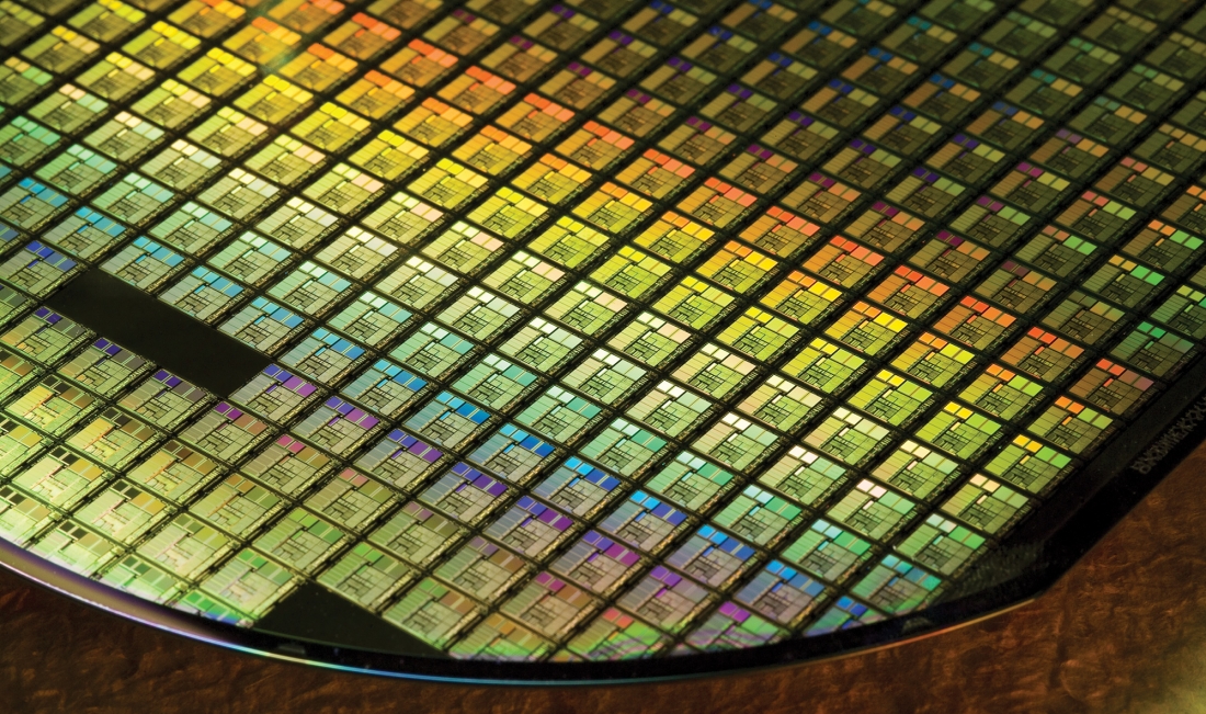
Developing almost unimaginably small transistors has driven the majority of advances in technology over the past decade. Now that hitting physical limitations of semiconductor materials is a valid concern and the difficulty is going up, chip makers are slowing down on their push towards sub-10nm processes.

To be clear, high performance chips have every reason to use smaller process nodes. However, the billions of chips produced that are not high-end CPUs or specialty processing chips will not be using processes smaller than 10nm for several more years. Fabless chip designers are now concerned that using smaller transistors could be too expensive to justify compared to 14nm and 12nm technologies that have high yields and well proven performance.

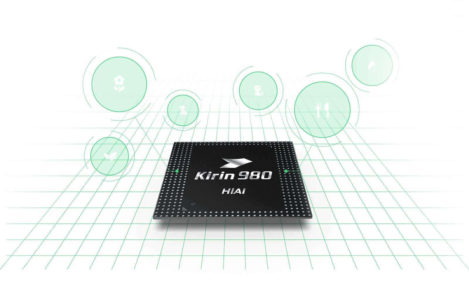
HiSilicon is Huawei's subsidiary company behind the world's first 7nm SoC for smartphones. Having already built out infrastructure for 10nm chips, the manufacturer has said that $300 million was spent to build its first 7nm SoC. It is unknown what the tooling costs are for mass production, but it is undoubtedly expensive. Low volume custom 7nm chips are clearly out of the question for the foreseeable future.

Qualcomm and MediaTek have both moved their 7nm chip launches into 2019. Both companies will still be aiming to deliver 7nm components for 5G networking equipment, but are waiting a little longer to avoid some of the difficulties of working with a process still early in its life cycle.

Samsung Electronics and TSMC are the only two pure-play foundries that have shared their 7nm plans. GlobalFoundries has decided to cease further development of 7nm FinFETs causing AMD to change partners. Instead of racing towards smaller nodes, GlobalFoundries is aiming to collect profits on higher margin 14nm chips that are in high demand.

Permalink to story.

 
I know there is a huge range of 'chips', but cpu-wise I recall Intel saying they would hit 10+ GHz, but that failed as their cpu's became space heaters, then the push to more cores and die shrink, but now that seems to be in difficulty. Intel also seems to have architecture problems with all the exploits being found, does anyone that knows about this stuff know where perhaps we will be seeking progress near term?
 
I know there is a huge range of 'chips', but cpu-wise I recall Intel saying they would hit 10+ GHz, but that failed as their cpu's became space heaters, then the push to more cores and die shrink, but now that seems to be in difficulty. Intel also seems to have architecture problems with all the exploits being found, does anyone that knows about this stuff know where perhaps we will be seeking progress near term?

After AMD/Qualcomm reach thier 7nm and after intel reaches production on their long awaited 10nm finfet (which is apparently similar to others 7nm in overall size) I suspect they will need to introduce a new material besides just silicon for their manufacturing to continue to make their transistors smaller. The 'architecture' problem is unrelated and is suppose to be solved at the hardware level in the 9xxx series (Whiskey Lake), currently it's microcode that patches these bugs. Near term, 10nm next year for intel, 7nm (Navi) next year for AMD.
 
I know there is a huge range of 'chips', but cpu-wise I recall Intel saying they would hit 10+ GHz, but that failed as their cpu's became space heaters, then the push to more cores and die shrink, but now that seems to be in difficulty. Intel also seems to have architecture problems with all the exploits being found, does anyone that knows about this stuff know where perhaps we will be seeking progress near term?

Slow progress to 5nm/3nm EUVL in maybe 3-5 years I would say. A few more trick techniques like gate all around FET will get only the richest companies there. Samsung, Intel, TSMC. That's it. Maybe they won't all make it below 7nm either.

Then lacking anything better short term some kind of 3D chip stacking or focus on interconnect technology to daisy chain and scale performance better. At the moment there are challenges for these techniques but they could be overcome if manufacturers started to focus on them more. 3D NAND is basically the thinking there. You need far better ways to connect the layers for complex processors like CPU and GPUs though, and potentially some kind of micro cooling channels between them as well.

The cost of developing and producing these technologies against just increasing 2D transistor density has held back the need to go down that route. Presented with few options beyond 5nm EUVL it will suddenly become much more interesting for the high end.

It's difficult to predict what technology will win long term because well.....none of the options are ideal just yet. Maybe it is use of a material or technique that does not exist yet. A fundamental change in computing might be required.

I am sure there will be a few breakthroughs though as long as the demand exists. All I see for certain is the time to find gains on silicon lithography will only keep lengthening.
 
Last edited:
Can someone please enlighten me. I'm curious what happens beyond after 1mn. It cannot shrink down further than that can it?

Will there be some sort of breakout design after?
 
Can someone please enlighten me. I'm curious what happens beyond after 1mn. It cannot shrink down further than that can it?

Will there be some sort of breakout design after?

You mean nm, not mm. And yes, you can go much smaller than 1nm. If you are using singular atoms as the structure, Helium has a diameter of 0.031nm. The hard part is finding an atom with a small size and the right properties. Even smaller then that are quarks.

Helium (the Alpha particle) is actually even smaller than that; .031nm is the boundary of its charge field, not the protons/neutrons/electrons themselves. Quarks don't exist and that's why all tech relating to them has gone nowhere.

Instead, as engineering catches up to modern physics and charge-channeling, we'll be moving to the photon level, not the atomic level. Photons are billions of times smaller than the proton, and of course move at light speed - much faster than the charge-blasted electrons in current architectures. Photon transistors will be the next great leap forward. The bottlenecks will then switch to any parts still using electrons, be it in the memory or motherboard or GPU connections.

Charge physics tells us that the photon is the mechanism that causes the E/M field, with electricity being charge moving axially through the nucleus and magnetism is charge emitting equatorially (with a cohered spin) from the nucleus, and the electrons are just along for the ride in the charge (photon) streams. That's why (as an example) electricity moves at light-speed minus impedance, while electrons of course move far, far slower. Engineers have yet to apply charge theory and mechanics in the lab, but they'll get there soon. It's becoming much more widely-accepted as the theory continues to dominate all data, again and again, and in almost every scientific field from geology to cosmology to medicine and botany.
 
Photons have no size, nobody ever measured the photon's cross-section.
Electron velocity in copper or other conducting media is irrelevant: electrical signals propagate at near speed light, depending on dielectric characteristics, so light signals do not have an advantage in this respect. Electrical signals are distorted by parasitic capacitance and inductances, so even if they propagate at near light speed the signal rise time at the far end is much longer than for light signals through transparent media.
In the end electrical signals and light are both E/M fields, that is photons, at different frequency or photon-energy.
 
It's becoming much more widely-accepted as the theory continues to dominate all data, again and again, and in almost every scientific field from geology to cosmology to medicine and botany.

Please don't mention medicine together with other sciences. Medicine is so outdated and backwards, it's not fully using even technology that was invented 80 years ago, let alone newer. If they started to use computational chemistry, they would have already find the cures for almost all diseases.

Instead, they don't even know the answers to the simplest questions. Such as: "What's the cause of diabetes type 2". So either they don't want to find the cures, because a cured patient is not a customer anymore, or they are absolute morons who can't find anything no matter how many labs and trillions of dollars you give them.

And that's what should be repeated often regarding medicine:
  1. Are you imbeciles who can't find even the simplest answers?
  2. Or are you corrupt bastards who want to keep the patients permanently in the status of "patient".
My bet is on the option 2, since it's impossible that all the researchers are morons. And we also know how "honest" are pharmaceutical corporations, but also the doctors.

For those reasons please don't mention medicine in the above context. Their goal isn't to use the technology to cure the people. So no matter how good MRI device you give them, even if they find the problem, they won't be able to fix it.

It's almost useless to waste technology on them, until more transparency is introduced into medicine. The level of crime and incompetence in medicine is absolutely incredible.
 
Last edited:
Back