Why it matters: The transition from planar transistors to FinFET was enough to keep Moore's Law relevant for the last 10 years, but even that design is running out of steam. Gate-all-around transistors look promising for 3 nm and beyond, but that transition could be the costliest yet.
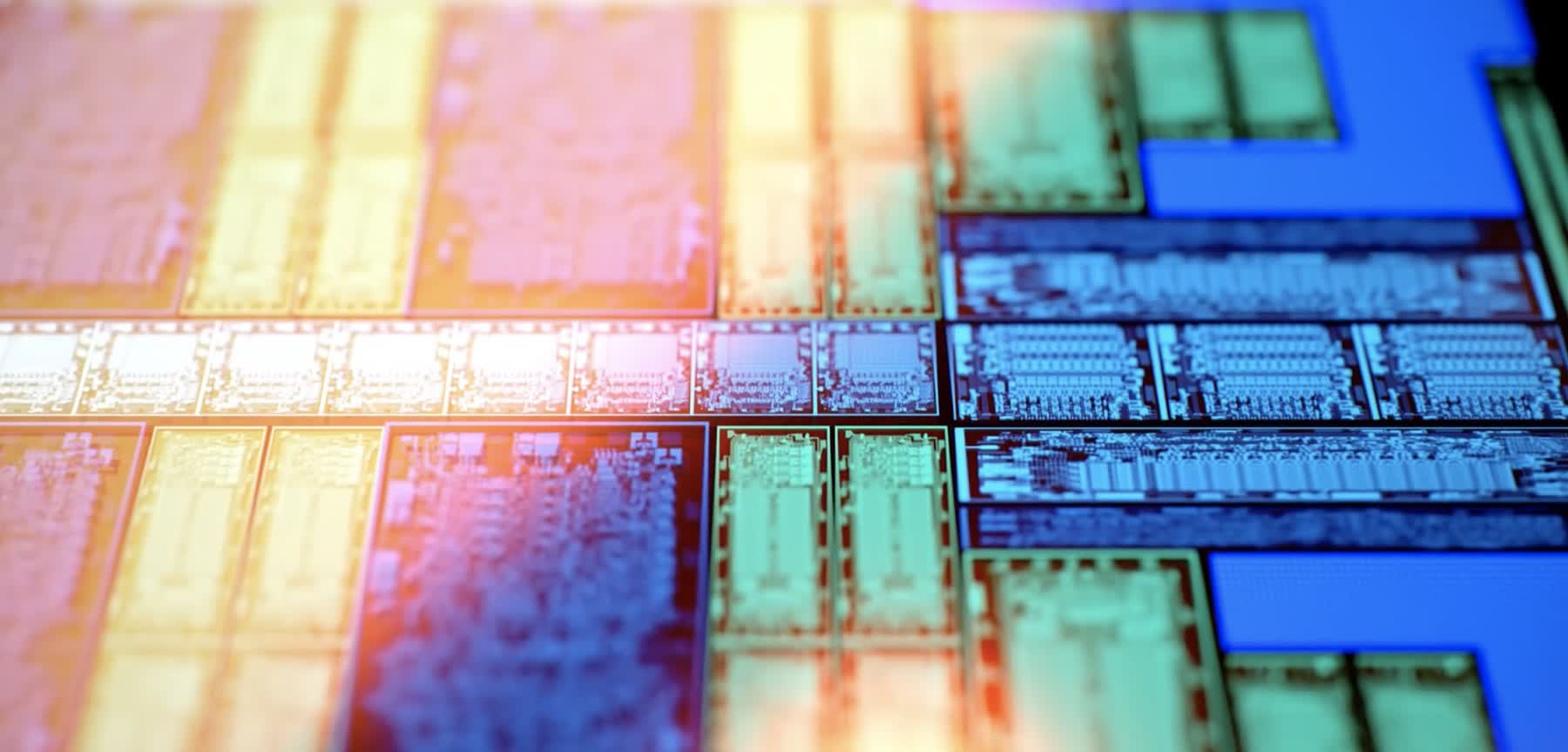
While most advanced chips today are manufactured on a 7 nm or 5 nm process node, large foundries like TSMC and GlobalFoundries have been busy developing newer nodes at 3 nm and 2 nm, based on next-generation, gate-all-around transistors (GAA-FET). Although GAA-FETs offer some advantages such as better scalability, faster switching times, better drive currents, and lower leakage, FinFET remains the preferred technology as manufacturers believe they can squeeze more out of it.
For example, TSMC said at the Technology Symposium last year that its N3 technology offers up to 50 percent better performance, up to a 30 percent reduction in power consumption, and more importantly, allows for 1.7 times the density of N5. Using a proven and more predictable process node will allow TSMC ample time to test GAA-FET for use at 2 nm. Last we've heard, the company planned to have a 2 nm process node ready for mass production by 2024.
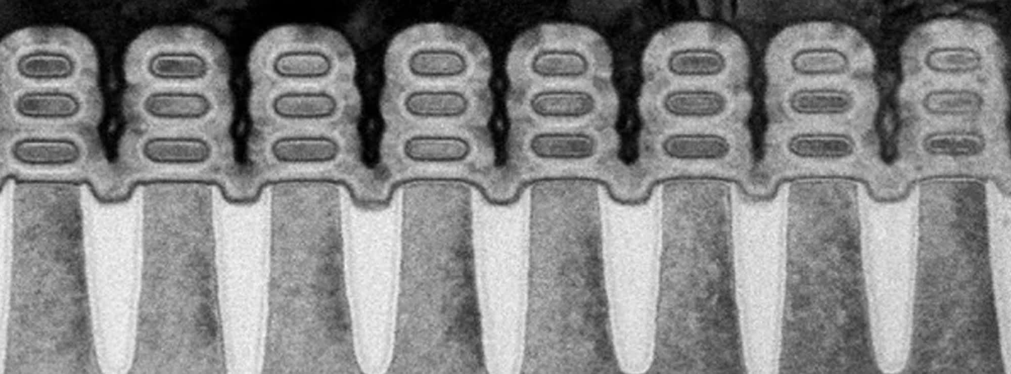
Image credit: Cross-section of GAAFET - IBM
According to a Semiconductor Engineering report, Intel and Samsung are also hard at work on transitioning to 3 nm and 2 nm nodes, and the latter could do so by the end of next year. There are multiple types of GAA-FET, and we know Samsung is planning to use nano-sheet-based MBC-FETs (Multi-Bridge Channel FET).
Essentially, MBC-FET is a FinFET turned on its side with the gate wrapped around nano-sheets of silicon grown on a substrate. Intel has a similar implementation based on "nanoribbons" planned for its 2025 chips, although this schedule could change under the new leadership.
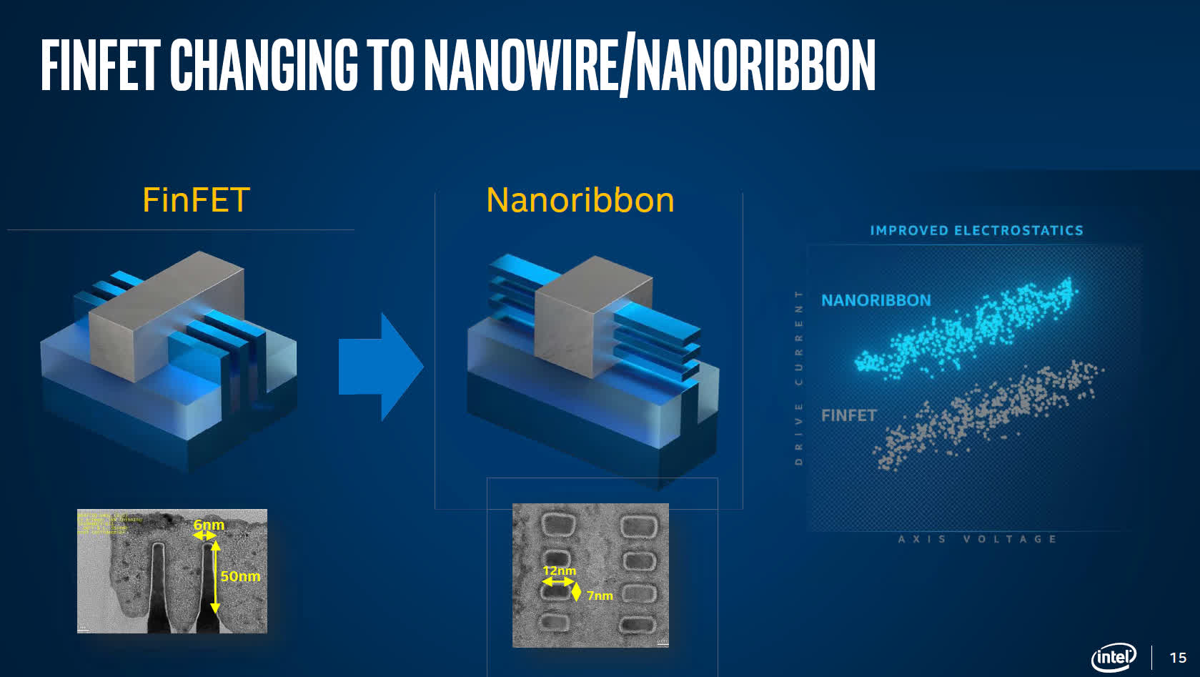
In any case, it looks like FinFET is on the way out, while foundries will have to adopt the GAA-FET for use beyond 3 nm process nodes. This isn't just the next transistor for advanced chips -- it might be the only option for the foreseeable future, with a few variations across foundries. The costs are also higher, which makes it unlikely that many foundries will afford the transition.
As things evolve, manufacturers may use high-mobility semiconductors like germanium, gallium antimonide, and indium arsenide to improve performance, but GAA-FET may be the last step in Moore's Law. That means manufacturers will have to get creative with advanced packaging and new chip architectures to keep the same cadence of progress.
https://www.techspot.com/news/88405-foundries-look-gaafet-new-process-nodes-beyond-3.html
